Hello! Welcome to Embedic!
FPGA is one of the physical implementations of digital circuits. Compared with ASIC chip, another important realization of digital circuit, an important feature of FPGA is its programmable feature, that is, the user can specify the FPGA to realize a specific digital circuit through the program.
In this article, we talk about FPGA from 5 aspects, what is FPGA, the FPGA architecture, FPGA design flow, the FPGA application and the difference between FPGA and ASIC, let's read on.
FPGA is a digital integrated circuit chip that can be used to write circuits, and is a chip used to design chips. You can use programming languages to design the circuits you want. In general, the circuit in the single-chip microcomputer has been solidified, and only the program needs to be input, while the FPGA is designed to use the programming language to design the circuit.
The working principle of Fpga is to adopt the concept of Logic Cell Array (LCA), which includes three parts: Configurable Logic Block (CLB), Input Output Block (IOB) and Interconnect.
A generic FPGA fabric consists of three types of modules. These are I/O blocks or pads, switch matrices/interconnects and Configurable Logic Blocks (CLBs). The basic FPGA architecture has a two-dimensional array of logic blocks with means for the user to arrange the interconnections between the logic blocks. The functions of the FPGA fabric blocks are discussed below:
A CLB (Configurable Logic Block) includes digital logic, inputs and outputs. It implements user logic.
Interconnects provide direction between logic blocks to implement user logic.
According to the logic, the switch matrix provides switching between interconnects.
I/O pads for the outside world to communicate with different applications.
Logic blocks contain MUXs (multiplexers), D flip-flops and LUTs. The LUT implements the function of combinational logic; the MUX is used to select the logic, and the D flip-flop stores the output of the LUT.
The basic building block of an FPGA is a look-up table-based function generator. The number of inputs to the LUT was varied from 3, 4, 6, and even to 8 after the experiment. Now, we have adaptive LUTs, each providing two outputs, and implementing two function generators.
The Xilinx Virtex-5 is the most popular FPGA and it contains a look-up table (LUT) connected to a MUX a flip-flop as described above. Today's FPGAs consist of roughly hundreds or thousands of configurable logic blocks. For configuring the FPGA, Modelsim and Xilinx ISE software were used to generate bitstream files and for development.
Field programmable gate arrays are divided into three categories based on applications such as low-end FPGAs, mid-range FPGAs and high-end FPGAs.
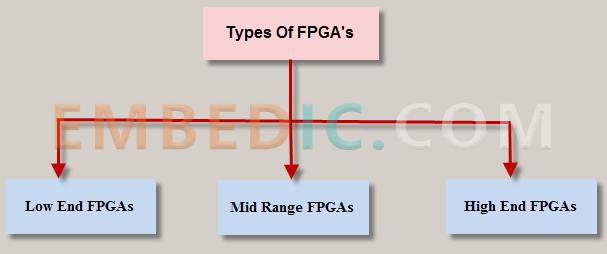
Low-end FPGA
These kinds of FPGAs are designed to be have low-power consumption, low-logic density, and low-complexity per chip.
For example, Altera's Cyclone series, Xilinx's Spartan series, and Lattice Semiconductor's Mach XO/ICE40.
Mid-range FPGA
These types of FPGAs are the best solution between low-end and high-end FPGAs, and they were developed to strike a balance between performance and cost. Examples of mid-range FPGAs are the Arria from Altera, the Artix-7/Kintex-7 series from Xlinix, the IGL002 from Microsemi and the ECP3 and ECP5 series from Lattice Semiconductor.
High-end FPGA
These sorts of FPGAs are established for reasoning density and also high performance. Instances of high-end FPGAs are Altera's Stratix series, Xilinx's Virtex series, Achronix's Speedster 22i series and Microsemi's ProASIC3 series.
FPGA development mainly includes nine parts, such as system design, design input, functional simulation, synthesis optimization, post-synthesis simulation, implementation and layout wiring, timing guidelines and verification, board-level guidelines and verification, and chip programming and debugging, as shown in the following figure.
1. Circuit Design: Before the system design, the first thing to do is the preparation work such as program demonstration, system design and FPGA chip selection.
2. Design input: The designed system or circuit hardware description language is represented and input to the EDA tool. Such as: Verilog HDL and VHDL, etc.
3. Functional Simulation: Functional simulation, also known as pre-simulation, is only the verification of the logic function of the circuit designed by the user, and there is no delay information in the simulation at this time, and only the preliminary function is checked. If an error is found, it returns to "design input" to modify the logic design.
4. Synthesis: Synthesis is the conversion of a high-level abstraction into a lower-level description. Synthesis optimization means compiling the design input into a logic connection netlist consisting of basic logic units such as gates, or gates, non-gates, RAM, flip-flops, etc., so as to optimize the generated logic connections and make the hierarchical design flat for implementation by FPGA layout and wiring software.
5. Post-synthesis simulation: Post-synthesis simulation is used to check whether the synthesis result is consistent with the original design. During simulation, the standard delay file generated by synthesis is back-labeled into the synthesis simulation model, and the impact brought by gate delay can be estimated. However, it is not yet possible to estimate the line delay, and the actual situation after layout wiring by a certain gap.
6. Implementation and Layout Wiring: Implementation is the configuration of the generated logic netlist to the specific FPGA chip, and the layout and wiring is one of the key steps. The layout process is to configure the hardware primitives and underlying units in the logic netlist to the inherent hardware structure inside the chip; the wiring is to use the various wiring resources inside the chip to connect each component reasonably and correctly according to the topology of the layout.
7. Timing Simulation and Verification: Timing simulation, also known as post-simulation, refers to the inverse marking of the delay information of the layout wiring into the design netlist to detect any timing violation.
8. Board-level simulation and verification: Board-level simulation is mainly used in high-speed circuit design to analyze the signal integrity, electromagnetic interference and other characteristics of the high-speed mind.
9. Chip programming and debugging: Chip programming means generating the data file (bit stream) to be use d, and then downloading the programming data to the FPGA chip, at which point the designer can debug and verify the system with an in-line logic analyzer (ILA).
FPGAs have enjoyed rapid growth over the past decade because they are suitable for a wide range of applications. specific applications for FPGAs include digital signal processing, bioinformatics, device controllers, software-defined radio, stochastic logic, ASIC prototyping, medical imaging, computer hardware simulation, integration of multiple SPLDs, speech recognition, encryption, filtering and communication coding, to name a few.
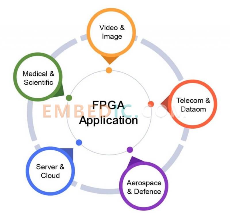
Typically, FPGAs are reserved for specific vertical applications with low production volumes. For these low-volume applications, top companies pay per unit of hardware cost. Today, new performance dynamics and costs have expanded the range of viable applications.
Some of the more common FPGA applications include: aerospace and defense, medical electronics, ASIC prototyping, audio, automotive, broadcast, consumer electronics, distributed monetary systems, data centers, high performance computing, industrial, medical, scientific instrumentation, security systems, video and image processing, wired communications, and wireless communications.
You may like: Microchip released the industry's first SoC FPGA development kit based on RISC-V instruction set architecture
An ASIC (Application Specific Integrated Circuit) is an IC that is designed with design usage in mind.
FPGA (Field Programmable Gate Array) is also an IC. as the name implies, with the right tools and proper professional foundation, engineers can reprogram the FPGA.
FPGA development is the use of HDL and quartus, vivado and other EDA tools to reconfigure (configure) the chip's functionality, while ASICs usually have less reconfigurable capabilities.
ASICs are basically designed based on standard cells to start with, and also require Place&Route. when there are any problems with the chip, it must be re-fed again until you achieve the functionality and performance you want. The ASIC style process is very costly and takes at least a couple of months to finish.
ASICs can never be changed after they leave the production line. That's why designers need to be completely sure the design is correct before mass production. Engineers can take advantage of the reconfigurability of FPGAs to prototype ASICs so that they can be fully tested in the real world before sending the design to the foundry.
ASICs have a big advantage in terms of repetitive cost because there is very little material wasted in the design. With FPGAs, there are always a lot of wasted hardware resources. This means that the repeat cost of FPGAs is usually higher than the repeat cost of similar ASICs.
While ASICs have very low repeat costs, their non-repeat costs are relatively high and usually in the millions. Since it is non-repetitive, the cost per IC decreases as the volume increases.
Therefore, after a certain volume of ASICs is produced, it can be cheaper to use ASICs than to use FPGAs. ASICs offer significant advantages over FPGAs in terms of power consumption, performance, size and cost.
Manufacturer: Texas Instruments
IC DGTL MEDIA SOC 337NFBGA
Product Categories: SOC
Lifecycle:
RoHS:
Manufacturer: Texas Instruments
IC DSP FIXED-POINT 196NFBGA
Product Categories: DSP
Lifecycle:
RoHS:
Manufacturer: Texas Instruments
IC DSP FIX/FLOAT POINT 841FCBGA
Product Categories: DSP
Lifecycle:
RoHS:
Manufacturer: Analog Devices
IC CCD SIGNAL PROCESSOR 88LFCSP
Product Categories: DSP
Lifecycle:
RoHS:
Looking forward to your comment
Comment
1
2
3
4
5
6
 Popular Searches
8 Bit MCU, Flash, PIC16 Family PIC16F7XX Series Microcontrollers, 20 MHz, 7 KB, 192 Byte, 44 Pi...
EEPROM 2K 256 X 8 2.5V SERIAL EE IND
System-On-Modules - SOM RCM2200
32-bit Arm Cortex-A53 vision processor with ISP, powerful 3D GPU, dual APEX-2 vision accelerat...
IC MCU 8BIT 60KB FLASH 44QFP
DSP 20MHZ 44QFP
Product updates, events, and resources in your inbox


Smart System

Traffic Management

Security

Consumer Electronics

Wireless Technology

Robot

Internet of Things

Industrial Control