Hello! Welcome to Embedic!
The STM32 F3 seriescombines a 32-bit ARM® Cortex®-M4 core (with FPU and DSP instructions) runningat 72 MHz with a high number of integrated analog peripherals leading to costreduction at application level and simplifying application design.
The above is a brief introduction to the STM32F3 series on the official website. As you can see, the STM32F3 arduino is a series of better performing MCUs from ST with enhanced peripherals that are part of the analog circuitry. For example, the STM32F303 has four operational amplifiers with programmable gain. The STM32F3 series of MCUs are not as widely used as the F4 series, so there is less online learning material available. embedic has gained some understanding of this series of MCUs after a short exposure. Now I will share some simple understanding of the operational amplifier (OPAMP) in the STM32F3 series (mainly STM32F303) chips to help more people. Since I have a STM32F3 DISCOVERY board from ST, the MCU model on it is STM32F303VCT6, so this article mainly targets the STM32F303 chip.
The main focus is on the chip's internal op-amp, so the resources of other chips will not be introduced too much, but a brief introduction to the chip's op-amp (OPAMP).
l 0.5mA output capability
l Rail-to-rail input/output
l In programmable gain mode (PGA), the gain can be set to 2,4,8,16
The connection of the input outputs of the operational amplifier to the IO of the MCU can be found in the MCU user manual, and the connection of the IO can also be found in the block diagram provided in the manual and is more graphic. Here is an example of an op-amp module in the STM32F303 to see how it is connected.
.jpg)
Part of STM32F303 internal op amp block diagram
Look mainly at the part in the red box, the ladder can be seen as a selector for multiple inputs and one output. We can see that for OPAMP1, there are four IO ports to choose from for the in-phase inputs, PA1,PA3, PA5, PA7 (note: according to the manual, "The external gainsetting mode gives full flexibility to According to this statement I think any one of the four IO ports can be multiplexed, as determined by the program). PA5 can be multiplexed as an output of the chip's internal DAC, and PA7 can also be multiplexed as an in-phase input of OPAMP2. For OPAMP1, its inverting input can be one of PA3, PC5. As can be seen from the diagram, the output of OPAMP1 can be connected directly to the chip's internal ADC module as an input to the ADC, and PA2 can also be multiplexed as its output. From this block diagram the connection of the modules inside the chip can be clearly seen, which helps a lot in the application of the MCU.
If the output of the on-chip op-amp is used as the input of the on-chip ADC, both the ADC and the op-amp need to be enabled, and the connection between the op-amp and the ADC is fixed, for example, the output of OPAMP1 is connected to channel3 of the on-chip ADC1.
The next three modes of operation of the op-amp are the application of the on-chip op-amp.
Standalone mode (external gain adjustment module)
Standalone mode (external gain setting mode)
Voltage following mode
l programmable gain mode
3.1 Standalone mode
The picture above shows the op-amp in standalone mode. For the purpose of illustration, the actual working circuit is outlined in red (as shown in the lower part of the picture). It is of course possible to connect it to other forms of amplification circuits.
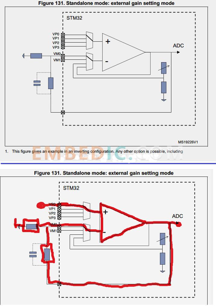
Illustrative diagram when the op amp is in standalone mode
3.2 Following Mode
In this mode the op-amp acts as a voltage follower with a gain of 1. For example, the in-phase input can be connected to the DAC to increase the output impedance of the circuit.
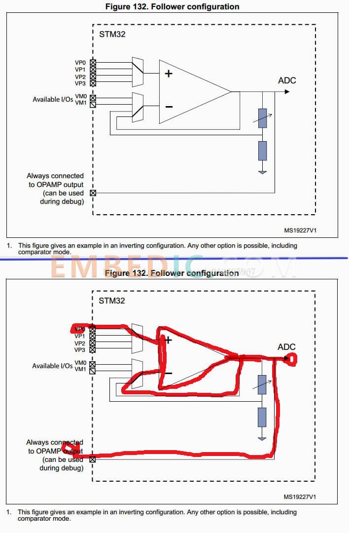
Illustration of voltage follow mode
3.3 Programmable Gain Mode
The gain can be selected from 2/4/8/16, or the op-amp can be used to make an active filter.
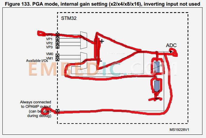
Illustration of Programmable Gain Mode
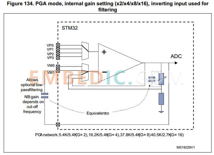
Op amp used as active filter
Manufacturer: Microchip
IC MCU 8BIT 32KB FLASH 40DIP
Product Categories: 8bit MCU
Lifecycle:
RoHS:
Manufacturer: ON Semiconductor
IC AUDIO PROCESSOR AD/DA 57CABGA
Product Categories: DSP
Lifecycle:
RoHS:
Manufacturer: Analog Devices
IC DSP 16/32B 400MHZ LP 176LQFP
Product Categories: DSP
Lifecycle:
RoHS:
Manufacturer: Analog Devices
IC DSP 16/32B 400MHZ LP 176LQFP
Product Categories: DSP
Lifecycle:
RoHS:
Looking forward to your comment
Comment
1
2
3
4
5
6
 Popular Searches
8 Bit MCU, Flash, PIC16 Family PIC16F7XX Series Microcontrollers, 20 MHz, 7 KB, 192 Byte, 44 Pi...
EEPROM 2K 256 X 8 2.5V SERIAL EE IND
System-On-Modules - SOM RCM2200
32-bit Arm Cortex-A53 vision processor with ISP, powerful 3D GPU, dual APEX-2 vision accelerat...
IC MCU 8BIT 60KB FLASH 44QFP
DSP 20MHZ 44QFP
Product updates, events, and resources in your inbox


Smart System

Traffic Management

Security

Consumer Electronics

Wireless Technology

Robot

Internet of Things

Industrial Control