Hello! Welcome to Embedic!
The PIC16F84A Microcontroller is a dual in-line (DIP) plastic package with a maximum clock frequency of 4MHz. Microchip PIC16F84A microcontroller has a central processing unit (CPU), program memory (ROM), data register (RAM) and two input/output ports (I/O ports). The CPU is the "brain" of the microcontroller, it reads and executes instructions from the program memory. When fetching and executing, the data register can also be fetched at the same time (PIC16F84A has been introduced with Harvard structure before). Program memory and data memory each have a bus connected to the CPU. The program memory of the PIC16F84A programmer is composed of Flash EPROM, which can be used for recording and erasing with electricity, and its contents can still be retained when the power is off. Some models of PIC microcontrollers use EPROM for program memory and need to be erased with ultraviolet light; some models are one-time programmable (OTP) products (it cannot be erased once programmed).
PIC16F84A has two input/output ports, namely A port and B port. Each pin of each port can be individually set as input or output. The bits of each port are numbered starting from 0. When port A is the output mode, its 4th bit (ie RA4) is an open collector (or open drain) output, while port B and other bits of port A are conventional full CMOS drive circuits. These functions must be paid attention to, otherwise errors will occur during programming. The CPU processes each port as 8 bits per byte, but port A has only 5 pins.
PIC input is compatible with COMS, so PIC output can drive TTL or CMOS logic chips. Each output pin can source or sink 20mA, even if only one pin is used at a time. PIC16F84A Circuit also has 64 EEPROM byte units for long-term storage of data, timer/counter modules, interrupt systems, etc.
In the Microcontrolador PIC16F84A, there are 68 bytes of general-purpose RAM with addresses from 0CH to 4FH. In addition to general-purpose data registers, there are some special registers, among which the most commonly used working register is the "W register". The CPU stores the working data in the W register. The function of register W is similar to "accumulator A" in other microcontrollers. In addition, there are several special registers, which control the operation of PIC in a certain way.
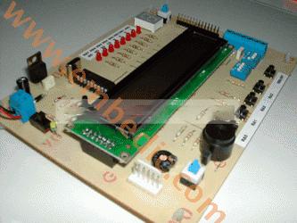
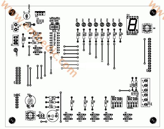
This is a new design based on the popular PIC16F84A Programming microcontroller tutorial board. It has 8 single LEDs, 7-segment display, LCD display and five buttons. This is an ideal solution for the beginner to take/her the first programming step in the world of microcontrollers. There is an in-circuit programming (ICP) header, which can be easily reprogrammed without having to unplug the PIC16F84A Circuit Diagram microcontroller every time. Programmers are provided to support this function.
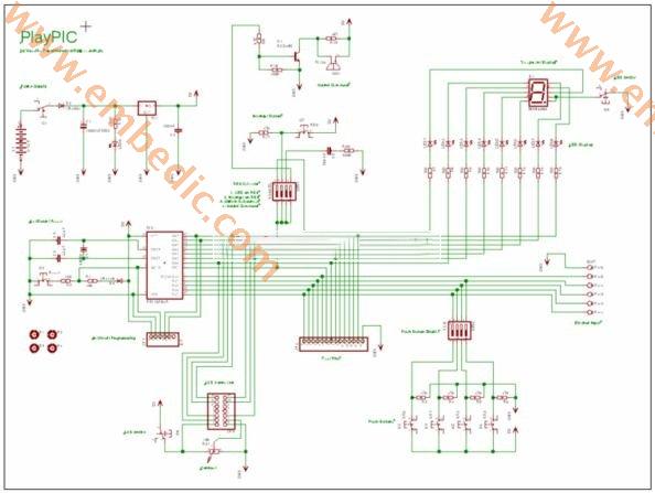
-When the S1 switch board is turned on and off, the LED indicator LED9 lights up
- S2 resets the microcontroller.
- S8 switch LCD display and off
-S9 switch has eight individual LEDs and seven segment display and off.
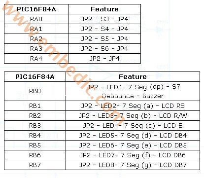
-Button S3, S6 corresponding to RA0-RA3 are turned on. Their SW2 DIP switch enables or disables.
-SW1 DIP switch enables or disables the following features:
1. Connect RB0 (as output) to LED1.
2. Connect RB0 (used as interrupt input) to S7
3. Enable the interrupt switch S7 debounce circuit.
4. Connect RB0 (as output), buzzer.
DIP switch must be 1000 or 0100 or 0110 or 0001.
-The 7-segment display is always connected to a single LED. Its seven subdivisions correspond to LED1 (RB0), LED2, LED8 (RB1 to RB7) and the decimal point. This correspondence can work together. It is a 7-segment display connected to the RB0 interrupt switch S7.
- JP4 is a 6-screw RA0-RA4 external input interface. When using, the corresponding input switches S3-S6 must be closed by SW2. Finally screw the ground.
- JP2 is a 14-pin test terminal. A voltmeter or logic analyzer can be connected to monitor the signal flow in the circuit at any time. The last pin is grounded
- JP1 is the ICP header. When circuit programming is executed, the board must be closed (S1), as well as LCD (S8) and LED (S9)
- JP3 is a 14-pin connector, LCD module. Contrast can be adjusted to fine-tune R21.
-The board can be powered by a 9V battery or a 6-12 V power supply.
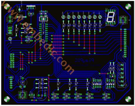
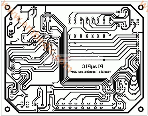
includes the PDF version of the schematic and PCB. The board has been successfully constructed and it is based on the following description
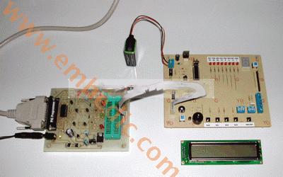
The photo below shows the help of the ICP header in the circuit programming procedure with the proper programmer function. In order for the program to work normally, the LCD module must be disconnected from the socket during the programming process.
Manufacturer: Microchip
IC MCU 32BIT 128KB FLASH 64QFN
Product Categories: 32bit MCU
Lifecycle:
RoHS:
Manufacturer: Texas Instruments
IC DSP FIXED-POINT 196NFBGA
Product Categories: DSP
Lifecycle:
RoHS:
Manufacturer: Texas Instruments
IC DGTL MEDIA PROCESSOR 337NFBGA
Product Categories: DSP
Lifecycle:
RoHS:
Manufacturer: Texas Instruments
IC DSP FIXED-POINT 688FCBGA
Product Categories: DSP
Lifecycle:
RoHS:
Looking forward to your comment
Comment
1
2
3
4
5
6
 Popular Searches
8 Bit MCU, Flash, PIC16 Family PIC16F7XX Series Microcontrollers, 20 MHz, 7 KB, 192 Byte, 44 Pi...
EEPROM 2K 256 X 8 2.5V SERIAL EE IND
System-On-Modules - SOM RCM2200
32-bit Arm Cortex-A53 vision processor with ISP, powerful 3D GPU, dual APEX-2 vision accelerat...
IC MCU 8BIT 60KB FLASH 44QFP
DSP 20MHZ 44QFP
Product updates, events, and resources in your inbox


Smart System

Traffic Management

Security

Consumer Electronics

Wireless Technology

Robot

Internet of Things

Industrial Control