Hello! Welcome to Embedic!
Today embedic.com will share with you the on-board resources of STM32F103RCT6, hoping to give some enlightenment to students who are new to STM32. If there is anything wrong with the discussion, you are welcome to go to https://www.embedic.com/ for questions and discussions.
The ALIENTEK MiniSTM32 V3 development board chooses STM32F103RCT6 as the MCU. Its resources include: 48KB SRAM, 256KB FLASH, 2 basic timers, 4 general-purpose timers, 2 advanced timers, 2 DMA controllers (total 12 channels), 3 SPIs, 2 IICs, 5 serial ports, 1 USB, 1 CAN, 3 12-bit ADCs, 1 12-bit DAC, 1 SDIO interface and 51 general-purpose IO ports. The STM32F103RCT6 development board schematic is extremely cost-effective. The schematic diagram of the MCU part is shown in the figure below:
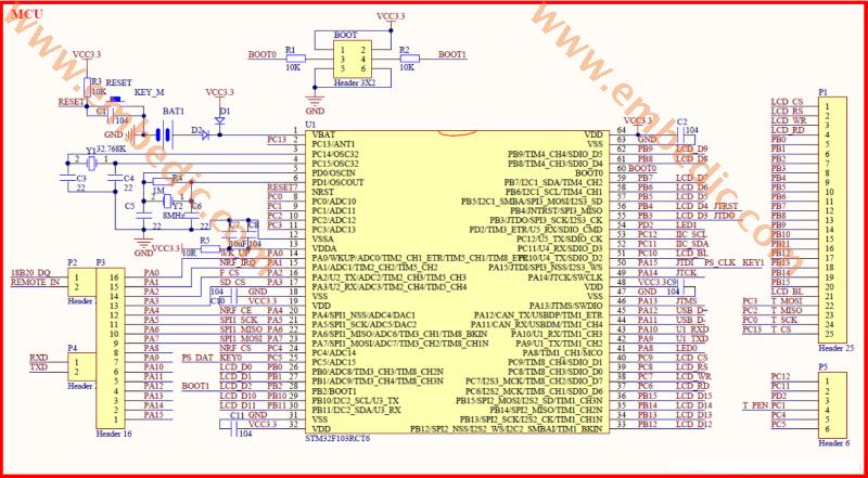
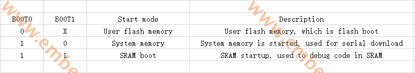
BOOT1 in the upper middle of the above figure is used to set the startup mode of STM32, and its corresponding startup mode is shown in the following table:
Under normal circumstances (that is, the standard ISP download procedure), if we want to use the serial port to download the code, we must first configure the STM32F103RCT6 schematic BOOT0 to 1, BOOT1 to 0, then press the reset button, and finally download the code through the program. Set BOOT0 to GND so that user code can be run after each reset. It can be seen that this standard ISP procedure is still very cumbersome. The jumper cap jumps around and needs to be reset manually. Therefore, ALIENTEK specially designed a one-key download circuit for the STM32 serial port download. Through the DTR and RTS signals of the serial port, To automatically control RST (reset) and BOOT0, so there is no need for the user to manually switch the state, the serial port download software is automatically controlled, and the code can be downloaded very conveniently, which is not available in other development boards.
The ALIENTEK MiniSTM32 development board comes with the 24C02 EEPROM chip. The chip's capacity is 2Kbit, which is 256 bytes. The schematic diagram is as follows:
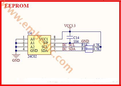
Ground A0~A2. For 24C02, set the address bit to 0. Pay attention to this when writing programs. IIC_SCL is connected to PC12 of MCU, and IIC_SDA is connected to PC11 of MCU. Here I did not connect to the IIC inside the STM32. If you want to use the hardware IIC on the STM32F103RCT6 arduino development board, then it is also possible. You only need to set PC11 and PC12 as floating inputs, and then set PB10 and PB11 (IIC2) or PB6 and PB7 (IIC1) are connected to PC11 and PC12 via flying leads to use hardware IIC.
The ALIENTEK MiniSTM32 development board has a total of 3 buttons, the schematic diagram is as follows:
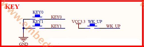
The WK_UP button is connected to PA0 (WKUP pin of STM32). In addition to being used as a normal input button, STM32F103RCT6 can also be used as a wake-up input for STM32. This button is triggered at high level. Since PA0 is also the input pin of DS18B20 and 18B20 has a pull-up resistor, when using the WK_UP button, please be sure to disconnect the jumper caps of PA0 and DS18B20.
KEY0 and KEY1 are used as normal key inputs and are connected to PC5 and PA15 respectively.
There are a total of 3 LEDs on the ALIENTEK MiniSTM32 development board. The schematic diagram is as follows:
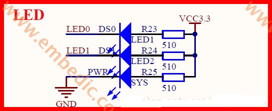
PWR is the power indicator of the development board, which is blue. LED0 and LED1 are connected to PA8 and PD2 respectively. PA8 can also control the brightness of DS0 through the PWM output of channel 1 of TIM1. DS0 is red, DS1 is green. The green light cannot achieve the breathing light.
The ALIENTEK MiniSTM32 development board is equipped with the SPI FLASH chip W25Q64, which has a capacity of 8M bytes. The schematic diagram is as follows:

The ALIENTEK MiniSTM32 development board is equipped with a USB serial port and powered by USB, so that we only need a USB cable to use the ALIENTEK MiniSTM32 development board, including serial port downloading code, power supply, and serial communication. The power supply part of the development board also leads to 5V (VOUT2) and 3.3V (VOUT1) headers, which can be used to provide power for external devices or introduce power from outside. This is very useful in many times. Sometimes you suddenly need a 3.3V power supply, but there is no such power supply for a long time, and the board can directly provide 3.3V power to the outside. With it, you can supply it to the outside The device provides 3.3V, 5V power supply. The USB interface (USB) of the development board is led out through an independent Mini USB header and is not shared with the USB to serial port (USB_232), so that it can not only be used at the same time, but also can provide greater current to the system.
The schematic diagrams of these parts are as follows:
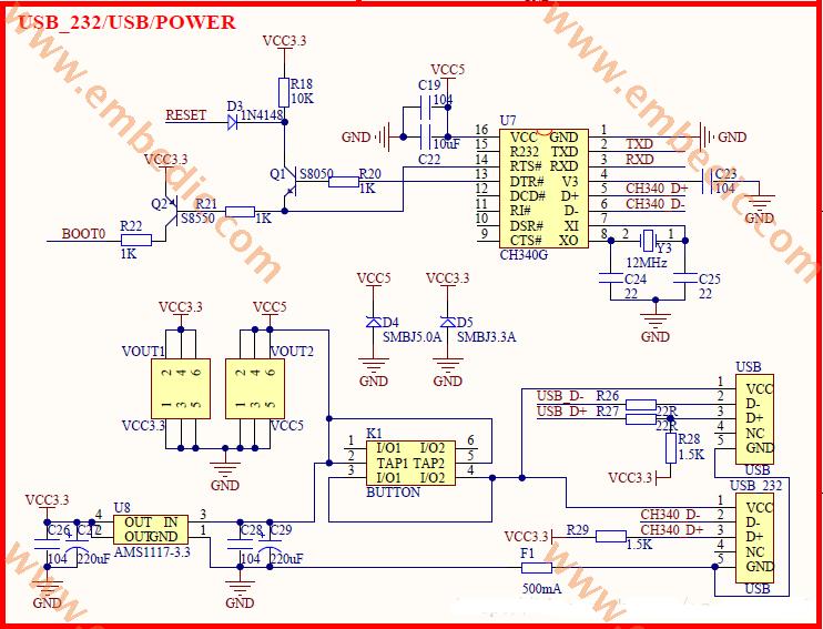
In the figure, Q1 and Q2 plus a few resistors and a diode constitute the one-key download circuit of the development board. This circuit uses RST and DTR signals to control the BOOT0 and RESET signals to realize the one-key download function. The specific implementation process of the one-key download circuit: First, mcuisp controls DTR to output low level, then DTR_N outputs high, and then RTS is set high, then RTS_N outputs low, so that Q2 is turned on, BOOT0 is pulled high, and BOOT0 is set to 1. At the same time, Q1 will be turned on, and the reset pin of STM32 will be pulled low to realize reset. Then, after a delay of 100ms, mcuisp controls DTR to be high, then DTR_N outputs low level, and RTS maintains high level, then RTS_N continues to be low level.
At this time, the reset pin of STM32, because Q1 is no longer conducting , Goes to high level, STM32 finishes resetting, but BOOT0 remains at 1, thus entering ISP mode, then mcuisp can start to connect to STM32, download the code, so as to realize one-key download. In addition, there is a switch K1 in this part to control the power supply of the whole system. If it is disconnected, the 3.3V part of the whole system will be powered off. The power of the 5V part is still on. In the figure, F1 is a recoverable fuse to protect the USB. The two TVS tubes D4 and D5 in the picture are used to protect the development board and prevent external high voltage pulses/static electricity from damaging the components on the development board.
Manufacturer: Texas Instruments
IC DSP FIXED POINT 196NFBGA
Product Categories: DSP
Lifecycle:
RoHS:
Manufacturer: Analog Devices
IC DSP CONTROLLER 32BIT 225BGA
Product Categories: 32bit DSP
Lifecycle:
RoHS:
Manufacturer: Texas Instruments
IC DGTL MEDIA PROCESSOR 337NFBGA
Product Categories: DSP
Lifecycle:
RoHS:
Manufacturer: Microchip
IC MCU 8BIT 7KB FLASH 44QFN
Product Categories: 8bit MCU
Lifecycle:
RoHS:
Looking forward to your comment
Comment
1
2
3
4
5
6
 Popular Searches
8 Bit MCU, Flash, PIC16 Family PIC16F7XX Series Microcontrollers, 20 MHz, 7 KB, 192 Byte, 44 Pi...
EEPROM 2K 256 X 8 2.5V SERIAL EE IND
System-On-Modules - SOM RCM2200
32-bit Arm Cortex-A53 vision processor with ISP, powerful 3D GPU, dual APEX-2 vision accelerat...
IC MCU 8BIT 60KB FLASH 44QFP
DSP 20MHZ 44QFP
Product updates, events, and resources in your inbox


Smart System

Traffic Management

Security

Consumer Electronics

Wireless Technology

Robot

Internet of Things

Industrial Control