Hello! Welcome to Embedic!
The Intel 8086 is a 16-bit microprocessor chip designed by Intel in 1978 and is the originator of the x86 architecture. Soon after, Intel introduced the Intel 8088 (a microprocessor with 8 external data buses). It was based on the 8080 and 8085 designs and had a similar register set, but the data bus was expanded to 16 bits. The Bus Interface Unit gives the ExecuTIon Unit a 6-byte prefixed queue of bit instructions, so instruction fetching and execution are synchronized. Each memory cell can hold one byte (8 bits) of binary information.
The Intel 8086 microprocessor is a representative processor with which various subsequent microprocessors have remained compatible.
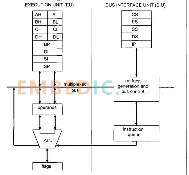
Instruction execution components EU
Performs 8-bit or 16-bit binary arithmetic and logic operations.
The operation results are sent to general-purpose registers or flag registers or written to memory.
Store the result characteristics of ALU operation or machine operation status.
Temporary storage of the operands participating in the operation, not programmable.
Four 16-bit data registers: AX, BX, CX, DX.
Four 16-bit address pointer and variable address registers: SP, BP, SI, DI.
Receives instructions from the BIU instruction queue and forms various timing control signals through instruction decoding to achieve specific timing operations for each EU component.
Bus Interface Unit BIU
Completes information transfer between CPU, memory, and I/O interface according to EU's request.
Providing fetching instructions from the memory to send to the instruction queue or directly to the EU for execution.
Fetch data from memory or peripheral to send to EU, or send the result of EU operation to memory or peripheral.
CS: Code Segment Register; DS: Data Segment Register; SS: Stack Segment Register; ES: Extended (additional) Data Segment Register.
Holds the offset address (effective address EA) of the next instruction to be executed.
Converts the 16-bit logical address into a 20-bit physical address of the access memory to complete the address addition operation.
Pre-stores 6 bytes of instruction code.
Sends bus control signals. Connects the 8086 CPU internal bus to the external bus.
8086 functionally divided into: execution component EU; bus interface component BIU
When there are 2 bytes free in the 8086 instruction queue, the bus interface part automatically prefetches instructions from memory into the instruction queue buffer.
When the EU component wants to execute an instruction, it takes out the instruction from the head of the instruction queue, and subsequent instructions are automatically advanced.
If the EU needs to access memory or I/O devices during instruction execution, the EU requests a bus cycle from the BIU and responds immediately if the BIU bus is free, or responds to the EU's bus request when the fetch operation is complete if the BIU is fetching an instruction.
When a transfer, call, or return instruction is encountered, the BIU automatically clears the existing contents of the instruction queue, starts from the new address of the transfer, call, or return, pre-reads the instruction from memory again, and fills the instruction queue.
These two parts neither work in a synchronous manner nor are they completely independent, but work in conjunction with each other.
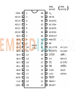
The 8086 CPU has 40 pins. It can be divided into 5 types of signals.
16-bit data lines: AD0 to AD15
20-bit address line: AD0 to AD19
Direct addressable space is 1M bytes. The address/data bus is time-division multiplexed. The rest are status lines, control signal lines, power supply, ground lines, etc.
16 address/data buses
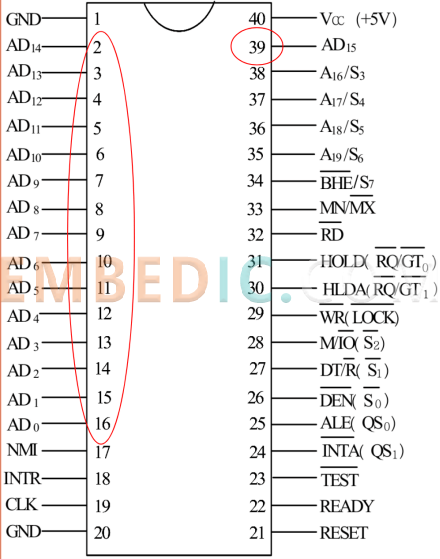
Four address/status lines
Nine control buses
RD (32, tri-state)
READY(22): "Ready" status signal input, active high. The "Ready" pin receives a "ready" status signal from the memory or I/O to the CPU. It indicates that the memory or I/O is ready for read/write operation. Coordinates the communication signal between the CPU and the memory or I/O for information transfer.
TEST(23): Test signal input, active low. TEST signal is used in combination with WAIT instruction, after the CPU executes WAIT instruction, it is in wait state, when TEST pin input low, the system is out of wait state and continues to execute the suspended instruction.
INTR(18): Maskable interrupt request signal input pin, introducing interrupt request signal from interrupt source to CPU, active high.
NMI(17) Non-maskable interrupt request signal input pin, active high. This signal is not affected by the state of interrupt allow flag IF, NMI has higher priority than INTR.
RESET(21): reset signal input, active high. After reset signal input, CPU ends the current operation and clears the processor's flag register, IP, DS, SS, ES registers and instruction queue, while setting CS to 0FFFFH.
CLK/(19): clock signal input, the clock frequency of 8086 CPU is 5MHz, that is, the frequency of the clock signal input from this pin is 5MHz.
MN/MX(33): min/max mode setting signal input pin.
Power and ground lines 3: VCC (40), GND (1, 20): power, ground pins, 8086 CPU uses a single +5 V power supply, there are two ground pins.
Q1. Why it is called 8086 microprocessor?
In June 1978, INTEL introduced the 8086 microprocessor with 4.77MHz main frequency, 16-bit registers, 16-bit data bus and 29,000 transistors of 3-micron technology, marking the third generation of microprocessors.
Q2. How many pins are there in 8086? How many pins does 8086 have?
40.
Q3. Is 8086 a RISC or CISC?
CISC.
Q4. What are Applications of 8086 Microprocessor?
1. Microcomputers are built using the 8086. For example, the IBM PC uses the Intel 8088, which is an 8086 version with an 8-bit data bus.
2. It is used in computers
3. It is used for control purposes, such as in traffic signals (using a microcontroller containing only one or more CPUs as well as memory and editable I/O peripherals)
Manufacturer: Texas Instruments
IC DSP FIX/FLOAT POINT 256BGA
Product Categories: DSP
Lifecycle:
RoHS:
Manufacturer: Analog Devices
IC DSP BLACKFIN 400MHZ 400CSBGA
Product Categories: DSP
Lifecycle:
RoHS:
Manufacturer: Texas Instruments
IC DGTL MEDIA PROCESSR 1031FCBGA
Product Categories: DSP
Lifecycle:
RoHS:
Manufacturer: Texas Instruments
IC DIGITAL MEDIA SOC 338NFBGA
Product Categories: SOC
Lifecycle:
RoHS:
Looking forward to your comment
Comment
1
2
3
4
5
6
 Popular Searches
8 Bit MCU, Flash, PIC16 Family PIC16F7XX Series Microcontrollers, 20 MHz, 7 KB, 192 Byte, 44 Pi...
EEPROM 2K 256 X 8 2.5V SERIAL EE IND
System-On-Modules - SOM RCM2200
32-bit Arm Cortex-A53 vision processor with ISP, powerful 3D GPU, dual APEX-2 vision accelerat...
IC MCU 8BIT 60KB FLASH 44QFP
DSP 20MHZ 44QFP
Product updates, events, and resources in your inbox


Smart System

Traffic Management

Security

Consumer Electronics

Wireless Technology

Robot

Internet of Things

Industrial Control