Hello! Welcome to Embedic!
Embedic.com uses LPC1768 to make a data acquisition device. Now I will summarize the experience in the design process and share with you.
LPC1768 development board is equipped with LPC1768 microprocessor (running speed up to 100MHz) and color TFT LCD display, 100M Ethernet, dual CAN, 2 serial ports, USB2.0 HOST/OTG/Device, SD/MMC interface.
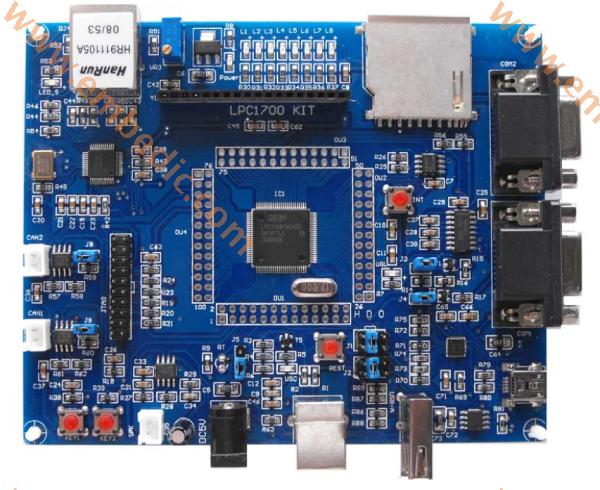
LPC1700 series chips use high-performance ARM Cortex-M3 V2 version 32-bit RISC core with a working frequency of 100 MHz. It has built-in high-speed memory (up to 512K bytes of flash memory and 64K bytes of SRAM), abundant enhanced I/O ports and peripherals connected to two APB buses. The board contains 8-channel 12-bit ADC and 10-bit DAC, 4 general-purpose 16-bit timers, motor control PWM interface, and multiple standard and advanced communication interfaces: up to 3 I2C, SPI, 2 I2S, 1 One SDIO, four USART, one USB Host/Device/OTG interface and two CAN, Ethernet MIC interfaces, Quadrature Encoder interface.
The rich peripheral configuration makes the LPC1700 microcontroller suitable for a variety of applications:
Motor drive and application control
Medical and handheld devices
Automotive electronics and other fields
Supports USB way to download the program. No JTAG or serial port is required, just a USB cable can download the program to FLASH. Convenient and fast.
Processor: NXPLPC1768, main frequency: 100MHz, 512KB FLASH Memory (on-chip), 64KB SRAM (on-chip)
AD (thermistor temperature measurement), DA (USB sound card) conversion.
Liquid crystal display (LCD12232, TFTLCD320X240 color screen interface).
USB2.0 interface, USB-HOST and USB OTG interface.
MMC/SD (SPI) interface (provide with FAT, FAT32 file system).
Two-way three-wire RS232 serial port.
Two-way CAN interface TJA1050.
RJ45-10/100M Ethernet network interface (PHY default: DP83848 can also provide DM9161AE driver to facilitate customers to change different PHY).
2 buttons, 8 LED lights. 2 function buttons-Reset and INT0 buttons.
Serial port ISP (bootloader) download function, JTGA debugging interface.
JTAG interface
IIC interface (AT24C16)
Other functions (speaker output driver-speakers can be connected directly).
The power supply is directly provided by an external regulated power supply or USB.
Four fixing holes are provided to facilitate users to install and fix.
Physical size: 130mm*105mm.
It adopts two-layer board process design, and is welded by the whole machine patch process, and the performance is reliable and stable.
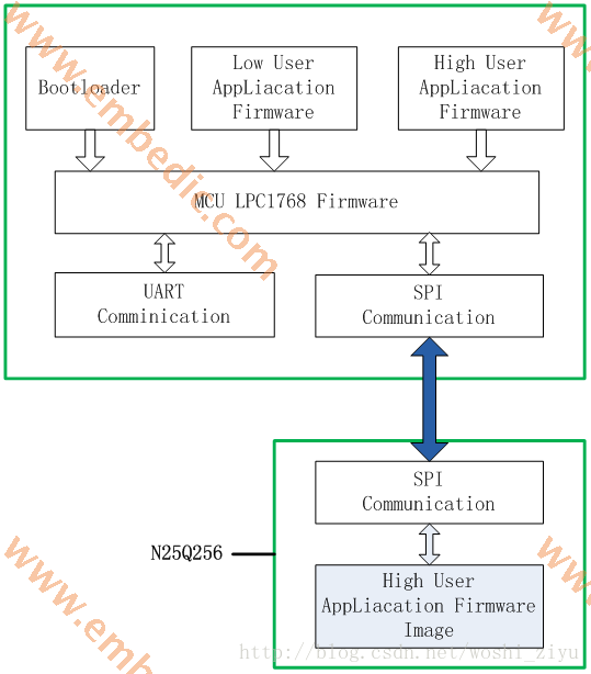
This solution is based on the LPC1768 Development Board as the platform, uses KEIL MDK4.70A as the development tool, and realizes the automatic update of the program through SPI.
The program program is composed of bootloader, low area user program, and high area user program. Bootloader realizes program jump and IAP program burning. The low area program is located at 0x1000~0x2FFFF of LPC1768, and the high area program is located at 0x30000~0x67FFFF of Mbed NXP LPC1768.
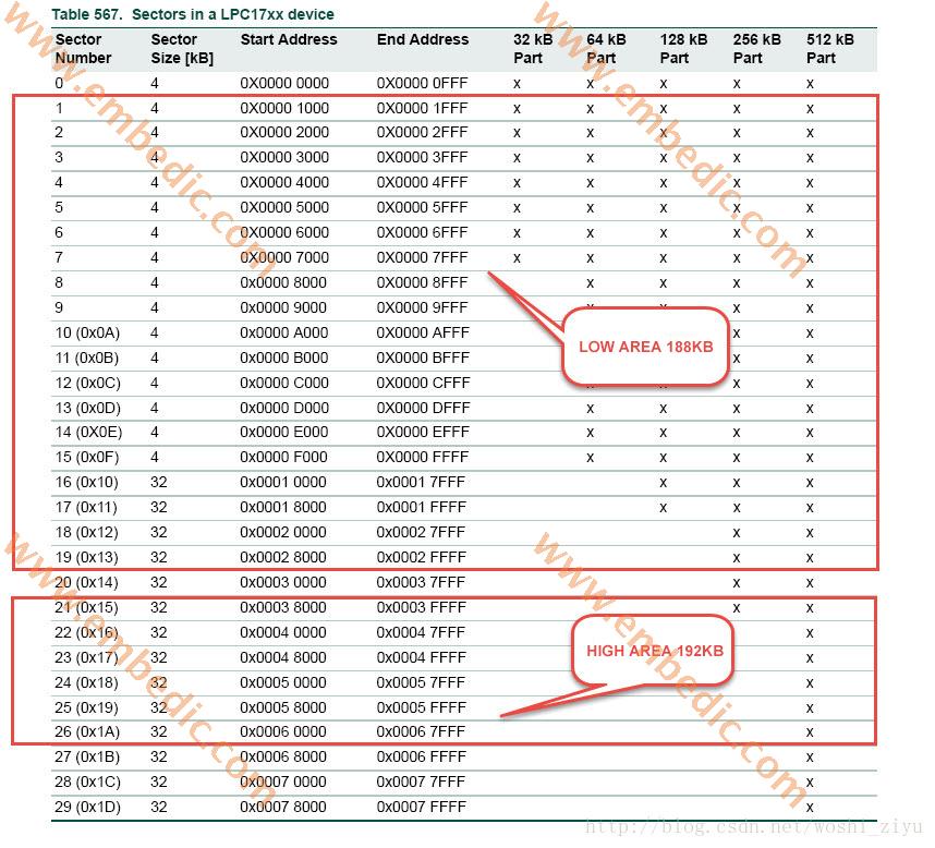
The program to be updated is placed at 0x00100000 of the external memory chip N25Q256 and occupies 48 sectors. The bootloader of LPC1768 Microcontroller reads the data of N25Q256 through SPI and updates the program to the user program of the high area. After the update is successful, the program is reset and the updated program is run.
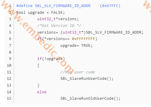
Bootloader mainly completes two functions, jump and IAP program burning. This program occupies the lowest 4K bytes of FLASH.
1. Program jump
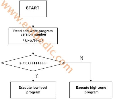
The last four bytes of the program in the high area (0x67FFC) store the version information of the program. The program jumps by judging the version information of the program in the high area. If the version information is 0xFFFFFFFF, the program in the high area is considered invalid and the program executes in the low area. User program, otherwise, execute high area program.
The program flow chart is as follows:
When jumping to the user program, use the function pointer to jump directly to the entry address of the user program.
Define function pointer:
typedef void (*USER_ENTRY_PFN)();
Define the program entry address:
#define SBL_SLV_FIRMWARE_START (0x38000)
user_entry = (USER_ENTRY_PFN) *((uint32_t*)(SBL_SLV_FIRMWARE_START + 4));
Realize the jump:
(user_entry)();
2. Upgrade procedure
The ascending program uses a scatter-loading mechanism to store the function pointer of the upgrade program in the lower 16 bytes of the program, that is, 0x00000FF0~0x00000FFF. After the user program receives the upgrade instruction, it uses the function pointer to jump to the entry address.
In the scatter-loading sct file, specify the FLASH space that stores the entry address of the function pointer:
LR_SBL_CODE 0x00000FF0 0x00000010{ ;SBL-API
ER_SBL0x00000FF0 0x00000010 { ;
sbl_slave.o("sbl_call", +First)
}
}
Specify the entry address of the function pointer
void SBL_APICall(uint32_t API, uint8_t*pData) __attribute__((section("sbl_call")));
In this way, the user program can jump to the bootloader by calling SBL_APICall.
3 Use IAP update program
IAP related functions and operating procedures can refer to NXP's routine files without modification.
Three, The user program needs to remap the interrupt vector.
Mbed LPC1768 remaps the interrupt vector by writing the offset in VTOR.
#defineVTOR_OFFSET (0x00038000)
__disable_irq();
SCB->VTOR = VTOR_OFFSET;
__enable_irq();
The program version number of the high area is located at address 0x67FFC, and the program version number will be updated when the code is programmed. Realized through the mechanism of scatter loading.
4, reference materials
1. AN11257: SPI secondary boot loader
The internal RTC configuration of LPC is relatively simple, and its initialization method is as follows:
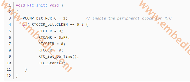
Get the time function. Here you need to build an RTC structure to store time data.
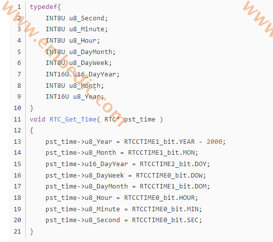
Also use this structure to initialize the time parameter
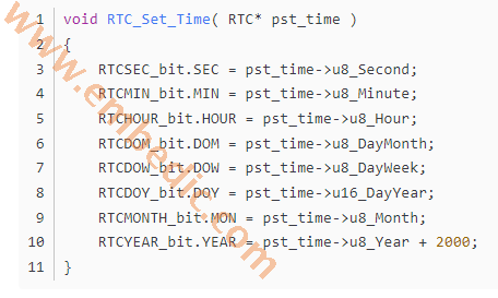
The configuration of RTC is completed through the above three functions.
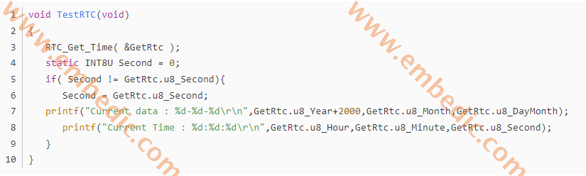
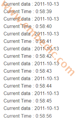
Test result: printed on the PC serial port monitoring software through uart interface.
RTC is a common component in current devices, and many devices need to check the time. The RTC real-time clock has been integrated in many single-chip microcomputers. Previously, a dedicated clock chip was required. Now the Cortex-M3 core includes this component. Unlike the previous ARM7 core of NXP, the clock source of the LPC1768 Board is only provided by the 32K clock source. This point should be noted, and the others are the same as ARM7.
RTC is actually a timer, which can be understood as a second timer. There are many RTC registers, but the register structure is relatively simple and it is very convenient to operate.
Explain several important registers, interrupt location register ILR, clock control register CCR, counter increment interrupt register CIIR, alarm mask register AMR
1. ILR interrupt location register
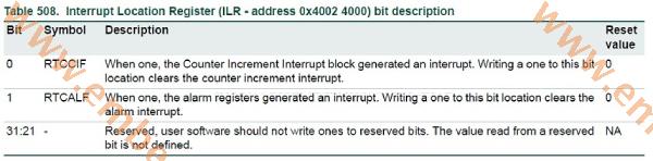
BIT0, when it is 1, the counter increment module generates an interrupt.
BIT1, when it is 1, the alarm register generates an interrupt
2.CCR clock control register
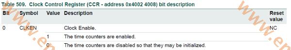
BIT0, clock time energy bit, 1 means time energy
BIT1, reset CTC.
BIT4, able to
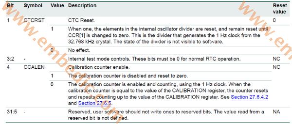
3.CIIR counter increment interrupt register
It can be clearly seen from the figure above that they respectively represent year, month, day, hour, minute and second, and the corresponding position is, and the corresponding interrupt is generated. The comparison is set to 0x01, which means an interrupt is generated every second, and it is set to 0x02, which means that an interrupt is generated every minute. .
4.AMR alarm mask register
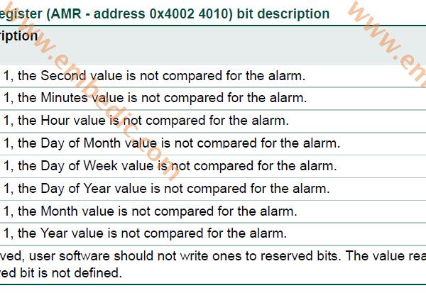
This register masks the corresponding alarm bit, which is the same as the CIIR bit definition.
As for other registers like year, month, day, hour, minute and second, the purpose of this register can be intuitively known, so I won’t describe them one by one.
Generate an interrupt every second, and send time data to the serial port in the interrupt.
Manufacturer: Texas Instruments
IC DSP FLOATING POINT 256BGA
Product Categories: DSP
Lifecycle:
RoHS:
Manufacturer: Texas Instruments
IC DSP FIXED POINT 257BGA
Product Categories: DSP
Lifecycle:
RoHS:
Manufacturer: Texas Instruments
IC DGTL MEDIA PROCESSOR 337NFBGA
Product Categories: DSP
Lifecycle:
RoHS:
Manufacturer: Texas Instruments
IC DSP FIXED-POINT 196NFBGA
Product Categories: DSP
Lifecycle:
RoHS:
Looking forward to your comment
Comment
1
2
3
4
5
6
 Popular Searches
8 Bit MCU, Flash, PIC16 Family PIC16F7XX Series Microcontrollers, 20 MHz, 7 KB, 192 Byte, 44 Pi...
EEPROM 2K 256 X 8 2.5V SERIAL EE IND
System-On-Modules - SOM RCM2200
32-bit Arm Cortex-A53 vision processor with ISP, powerful 3D GPU, dual APEX-2 vision accelerat...
IC MCU 8BIT 60KB FLASH 44QFP
DSP 20MHZ 44QFP
Product updates, events, and resources in your inbox


Smart System

Traffic Management

Security

Consumer Electronics

Wireless Technology

Robot

Internet of Things

Industrial Control