Hello! Welcome to Embedic!
This website uses cookies. By using this site, you consent to the use of cookies. For more information, please take a look at our Privacy Policy.
Home > Embedded ICs > Embedded - Memory > XC18V04VQ44I
Xilinx

XC18V04VQ44I

Pictures are for reference only Please prevail in kind
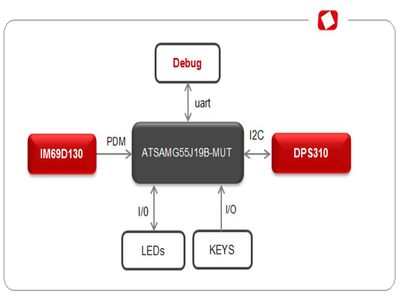
  • Quantity : *

  • Contact Name : *

  • Email : *

price SUPPLIERS WHOLESALE PRICE TRENDS

Price comparison from authorized distributors

price info XC18V04VQ44I Competitive Prices

EmbedIC has the unique source of supply. We can offer XC18V04VQ44I more competitive price for our customers. You can enjoy our best service by purchasing XILINX XC18V04VQ44I, Please feel free to contact for the best price of XC18V04VQ44I Memory. Click To Get Quotation

XC18V04VQ44I Overview

Features
• In-system programmable 3.3V PROMs for configuration of Xilinx FPGAs
  - Endurance of 20,000 program/erase cycles
  - Program/erase over full commercial/industrial voltage and temperature range (–40°C to +85°C)
• IEEE Std 1149.1 boundary-scan (JTAG) support
• Simple interface to the FPGA
• Cascadable for storing longer or multiple bitstreams

• Low-power advanced CMOS FLASH process


• Dual configuration modes
  - Serial Slow/Fast configuration (up to 33 MHz)
  - Parallel (up to 264 Mb/s at 33 MHz)
• 5V tolerant I/O pins accept 5V, 3.3V and 2.5V signals
• 3.3V or 2.5V output capability
• Available in PC20, SO20, PC44, and VQ44 packages
• Design support using the Xilinx Alliance and Foundation series software packages.

• JTAG command initiation of standard FPGA configuration


Description
Xilinx introduces the XC18V00 series of in-system programmable configuration PROMs (Figure 1). Devices in this 3.3V family include a 4-megabit, a 2-megabit, a 1-megabit, and a 512-kilobit PROM that provide an easy-to-use, cost-effective method for re-programming and storing Xilinx FPGA configuration bitstreams.
When the FPGA is in Master Serial mode, it generates a configuration clock that drives the PROM. A short access time after CE and OE are enabled, data is available on the PROM DATA (D0) pin that is connected to the FPGA DIN pin. New data is available a short access time after each rising clock edge. The FPGA generates the appropriate number of clock pulses to complete the configuration. When the FPGA is in Slave Serial mode, the PROM and the FPGA are clocked by an external clock.

When the FPGA is in Master-SelectMAP mode, the FPGA generates a configuration clock that drives the PROM.

When the FPGA is in Slave-Parallel or Slave-SelectMAP Mode, an external oscillator generates the configuration clock that drives the PROM and the FPGA. After CE and OE are enabled, data is available on the PROMs DATA (D0-D7) pins. New data is available a short access time after each rising clock edge. The data is clocked into the FPGA on the following rising edge of the CCLK. A free-running oscillator can be used in the Slave-Parallel or Slave-SelecMAP modes.

Multiple devices can be concatenated by using the CEO output to drive the CE input of the following device. The clock inputs and the DATA outputs of all PROMs in this Chain are interconnected. All devices are compatible and can be cascaded with other members of the family or with the XC17V00 one-time programmable Serial PROM family.


Features

  • In-System Programmable 3.3V PROMs for Configuration of Xilinx FPGAs
    • Endurance of 20,000 Program/Erase Cycles
    • Program/Erase Over Full Industrial Voltage and Temperature Range (–40°C to +85°C)
  • IEEE Std 1149.1 Boundary-Scan (JTAG) Support
  • JTAG Command Initiation of Standard FPGA Configuration
  • Simple Interface to the FPGA
  • Cascadable for Storing Longer or Multiple Bitstreams
  • Low-Power Advanced CMOS FLASH Process
  • Dual Configuration Modes
    • Serial Slow/Fast Configuration (up to 33 MHz)
    • Parallel (up to 264 Mb/s at 33 MHz)
  • 5V-Tolerant I/O Pins Accept 5V, 3.3V and 2.5V Signals
  • 3.3V or 2.5V Output Capability
  • Design Support Using the Xilinx ISE™ Foundation™ Software Packages
  • Available in PC20, SO20, PC44, and VQ44 Packages
  • Lead-Free (Pb-Free) Packaging

Specifications

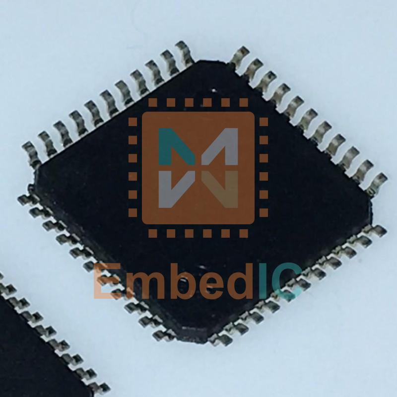
  • Mounting Style Surface Mount

  • Memory Size 500000 B

  • Product Lifecycle Status Obsolete

  • Packaging Bulk, Tube

  • Lead-Free Status Contains Lead

  • RoHS Non-Compliant

  • Supply Voltage (DC) 3.30 V, 3.60 V (max)

  • Case/Package 44-TQFP

Circuit Diagram

XC18V04VQ44I

Popular Products

  • CY95F633KPMC-G-SNE2

    Manufacturer: Cypress

    IC MCU 8BIT 12KB FLASH 32LQFP

    Product Categories: 8bit MCU

    Lifecycle:

    RoHS:

  • S912XD256F1CAA

    Manufacturer: Freescale

    16-bit Microcontrollers - MCU POR -40 C to + 85 C HCS12X MCU SCI

    Product Categories: 16bit MCU

    Lifecycle:

    RoHS:

Product evaluation

  • Looking forward to your comment

  • Comment

    Verification Code * 

Compare products

Compare Empty