Hello! Welcome to Embedic!

Pictures are for reference only Please prevail in kind
IC DPS FIXED-POINT 144-BGA
 PCB Symbol, Footprint
 Send Inquiry
 Download Datasheet
 SUPPLIERS WHOLESALE PRICE TRENDS
Price comparison from authorized distributors
 TMS320VC5401ZGU50 Competitive Prices
EmbedIC has the unique source of supply. We can offer TMS320VC5401ZGU50 more competitive price for our customers. You can enjoy our best service by purchasing Texas Instruments TMS320VC5401ZGU50, Please feel free to contact for the best price of TMS320VC5401ZGU50 DSP. Click To Get Quotation
The TMS320VC5401 fixed-point, digital signal processor (DSP) (hereafter referred to as the 5401 unless otherwise specified) is based on an advanced modified Harvard architecture that has one program memory bus and three data memory buses. This processor provides an arithmetic logic unit (ALU) with a high degree of parallelism, application-specific hardware logic, on-chip memory, and additional on-chip peripherals. The basis of the operational flexibility and speed of this DSP is a highly specialized instruction set.
Separate program and data spaces allow simultaneous access to program instructions and data, providing the high degree of parallelism. Two read operations and one write operation can be performed in a single cycle. Instructions with parallel store and application-specific instructions can fully utilize this architecture. In addition, data can be transferred between data and program spaces. Such parallelism supports a powerful set of arithmetic, logic, and bit-manipulation operations that can be performed in a single machine cycle. In addition, the 5401 includes the control mechanisms to manage interrupts, repeated operations, and function calls.
Clock Rate 50MHz
Operating Temperature -40℃ ~ 100℃ (TC)
Type Fixed Point
Non-Volatile Memory ROM (8 kB)
Package / Case 144-LFBGA
Voltage - Core 1.80V
Voltage - I/O 3.30V
Mounting Type Surface Mount
Interface Host Interface, McBSP
Supplier Device Package 144-BGA MICROSTAR (12x12)
On-Chip RAM 16kB
Manufacturer: Cypress
IC MCU 32BIT 160KB FLASH 48QFN
Product Categories: 32bit MCU
Lifecycle:
RoHS:
Manufacturer: STMicroelectronics
IC MCU 32BIT 512KB FLASH 100LQFP
Product Categories: 32bit MCU
Lifecycle:
RoHS:
Manufacturer: Microchip
IC MCU 16BIT 128KB FLASH 100TQFP
Product Categories: 16bit MCU
Lifecycle:
RoHS:
Manufacturer: Cypress
IC MCU 16B FFMC-16F-0.35 100QFP
Product Categories: General MCU
Lifecycle:
RoHS:
Manufacturer: Microsemi Corporation
IC SOC CORTEX-M3 166MHZ 256FBGA
Product Categories: SOC
Lifecycle:
RoHS:
Manufacturer: Microsemi Corporation
IC SOC CORTEX-M3 166MHZ 325BGA
Product Categories: SOC
Lifecycle:
RoHS:
Manufacturer: Microchip
IC MCU 8BIT 32KB FLASH 44QFN
Product Categories: 8bit MCU
Lifecycle:
RoHS:
Manufacturer: Microsemi Corporation
IC SOC CORTEX-M3 166MHZ 484FBGA
Product Categories: SOC
Lifecycle:
RoHS:
Looking forward to your comment
Comment
 Popular Searches
8 Bit MCU, Flash, PIC16 Family PIC16F7XX Series Microcontrollers, 20 MHz, 7 KB, ...
EEPROM 2K 256 X 8 2.5V SERIAL EE IND
System-On-Modules - SOM RCM2200
32-bit Arm Cortex-A53 vision processor with ISP, powerful 3D GPU, dual APEX-2 v...
IC MCU 8BIT 60KB FLASH 44QFP
DSP 20MHZ 44QFP
1
2
3
4
5
6
Product updates, events, and resources in your inbox


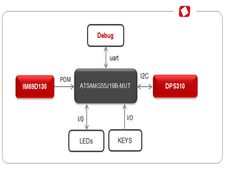
Smart System

Traffic Management

Security

Consumer Electronics

Wireless Technology

Robot

Internet of Things

Industrial Control