Hello! Welcome to Embedic!
This website uses cookies. By using this site, you consent to the use of cookies. For more information, please take a look at our Privacy Policy.
Home > Embedded ICs > Embedded - System On Chip (SoC) > TMS320DM365ZCE27
Texas Instruments

TMS320DM365ZCE27

Pictures are for reference only Please prevail in kind
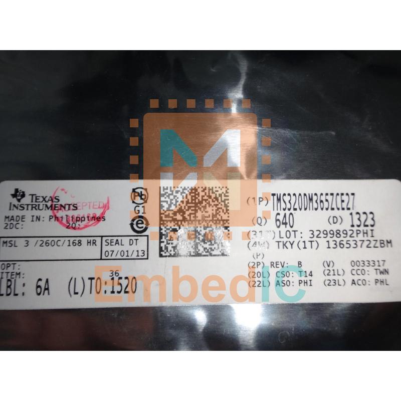
  • Quantity : *

  • Contact Name : *

  • Email : *

price SUPPLIERS WHOLESALE PRICE TRENDS

Price comparison from authorized distributors

price info TMS320DM365ZCE27 Competitive Prices

EmbedIC has the unique source of supply. We can offer TMS320DM365ZCE27 more competitive price for our customers. You can enjoy our best service by purchasing Texas Instruments TMS320DM365ZCE27, Please feel free to contact for the best price of TMS320DM365ZCE27 SOC. Click To Get Quotation

TMS320DM365ZCE27 Overview

Developers can now deliver pixel-perfect images at up to 720p H.264 at 30fps in their digital video designs without concerns of video format support, constrained network bandwidth, limited system storage capacity or cost with the new TMS320DM365 digital media processor based on DaVinci technology from Texas Instruments Incorporated (TI). With multi-format HD video, the DM365 also features a suite of peripherals saving developers on system costs.

This ARM9-based DM365 device offers speeds up to 300 MHz and supports production-qualified H.264, MPEG-4, MPEG-2, MJPEG and VC1/WMV9 codecs providing customers with the flexibility to select the right video codec for their application. These codecs are driven from video accelerators offloading compression needs from the ARM core so that developers can utilize the most performance from the ARM for their application. Video surveillance designers achieve greater compression efficiency providing more storage without straining the network bandwidth. Developers of media playback and camera-driven applications, such as video doorbells, digital signage, digital video recorders, portable media players and more can ensure interoperability as well as product scalability by taking advantage of the full suite of codecs supported on the DM365.

Along with multi-format HD video, the DM365 enables seamless interface to most additional external devices required for video applications. The image sensor interface is flexible enough to support CCD, CMOS, and various other interfaces such as BT.656, BT1120. The DM365 also offers a high level of integration with HD display support including, 3 built-in 10-bit HD Analog Video Digital to Analog Converters (DACs), DDR2/mDDR, Ethernet MAC, USB 2.0, integrated audio, Host Port Interface (HPI), Analog to Digital Converter, and many more features saving developers on overall system costs as well as real estate on their circuit boards allowing for a slimmer, sleeker design.

Features

  • Highlights
    • High-Performance Digital Media System-on-Chip (DMSoC)
    • Up to 300-MHz ARM926EJ-S Clock Rate
    • Two Video Image Co-processors (HDVICP, MJCP) Engines
    • Supports a Range of Encode, Decode, and Video Quality Operations
    • Video Processing Subsystem
      • HW Face Detect Engine
      • Resize Engine from 1/16x to 8x
      • 16-Bit Parallel AFE (Analog Front-End) Interface Up to 120 MHz
      • 4:2:2 (8-/16-bit) Interface
      • 8-/16-bit YCC and Up to 24-Bit RGB888 Digital Output
      • 3 DACs for HD Analog Video Output
      • Hardware On-Screen Display (OSD)
    • Capable of 720p 30fps H.264 video processing
      Note: 216-MHz is only capable of D1 processing
    • Peripherals include EMAC, USB 2.0 OTG,DDR2/NAND, 5 SPIs, 2 UARTs, 2 MMC/SD/SDIO, Key Scan
    • 8 Different Boot Modes and Configurable Power-Saving Modes
    • Pin-to-pin and software compatible with DM368
    • Extended temperature (-40°C - 85°C) available for 300-Mhz device
    • 3.3-V and 1.8-V I/O, 1.2-V/1.35-V Core
    • 338-Pin Ball Grid Array at 65nm Process Technology
  • High-Performance Digital Media System-on-Chip (DMSoC)
    • 216-, 270-, 300-MHz ARM926EJ-S Clock Rate
    • Fully Software-Compatible With ARM9
  • ARM926EJ-S Core
    • Support for 32-Bit and 16-Bit (Thumb Mode) Instruction Sets
    • DSP Instruction Extensions and Single Cycle MAC
    • ARM Jazelle Technology
    • EmbeddedICE-RT Logic for Real-Time Debug
  • ARM9 Memory Architecture
    • 16K-Byte Instruction Cache
    • 8K-Byte Data Cache
    • 32K-Byte RAM
    • 16K-Byte ROM
    • Little Endian
  • Two Video Image Co-processors (HDVICP, MJCP) Engines
    • Support a Range of Encode and Decode Operations
    • H.264, MPEG4, MPEG2, MJPEG, JPEG, WMV9/VC1
  • Video Processing Subsystem
    • Front End Provides:
      • HW Face Detect Engine
      • Hardware IPIPE for Real-Time Image Processing
        • Resize Engine
          • Resize Images From 1/16× to 8×
          • Separate Horizontal/Vertical Control
          • Two Simultaneous Output Paths
      • IPIPE Interface (IPIPEIF)
      • Image Sensor Interface (ISIF) and CMOS Imager Interface
      • 16-Bit Parallel AFE (Analog Front End) Interface Up to 120 MHz
      • Glueless Interface to Common Video Decoders
      • BT.601/BT.656/BT.1120 Digital YCbCr 4:2:2 (8-/16-Bit Module
      • Histogram Module
      • Lens distortion correction module (LDC)
      • Hardware 3A statistics collection module (H3A)
    • Back End Provides:
      • Hardware On-Screen Display (OSD)
      • Composite NTSC/PAL video encoder output
      • 8-/16-bit YCC and Up to 24-Bit RGB888 Digital Output
      • 3 DACs for HD Analog Video Output
      • LCD Controller
      • BT.601/BT.656 Digital YCbCr 4:2:2 (8-/16-Bit) Interface
  • Analog-to-Digital Convertor (ADC)
  • Power Management and Real Time Clock Subsystem (PRTCSS)
    • Real Time Clock
  • 16-Bit Host-Port Interface (HPI)
  • 10/100 Mb/s Ethernet Media Access Controller (EMAC) - Digital Media
    • IEEE 802.3 Compliant
    • Supports Media Independent Interface (MII)
    • Management Data I/O (MDIO) Module
  • Key Scan
  • Voice Codec
  • External Memory Interfaces (EMIFs)
    • DDR2 and mDDR SDRAM 16-bit wide EMIF With 256 MByte Address Space (1.8-V I/O)
    • Asynchronous16-/8-bit Wide EMIF (AEMIF)
      • Flash Memory Interfaces
        • NAND (8-/16-bit Wide Data)
        • 16 MB NOR Flash, SRAM
        • OneNAND(16-bit Wide Data)
  • Flash Card Interfaces
    • Two Multimedia Card (MMC) / Secure Digital (SD/SDIO)
    • SmartMedia/xD
  • Enhanced Direct-Memory-Access (EDMA) Controller (64 Independent Channels)
  • USB port with Integrated 2.0 High-Speed PHY that Supports
    • USB 2.0 High-Speed Device
    • USB 2.0 High-Speed Host (mini-host, supporting one external device)
    • USB On The Go (HS-USB OTG)
  • Four 64-Bit General-Purpose Timers (each configurable as two 32-bit timers)
  • One 64-Bit Watch Dog Timer
  • Two UARTs (One fast UART with RTS and CTS Flow Control)
  • Five Serial Port Interfaces (SPI) each with two Chip-Selects
  • One Master/Slave Inter-Integrated Circuit (I2C) Bus
  • One Multi-Channel Buffered Serial Port (McBSP)
    • I2S
    • AC97 Audio Codec Interface
    • S/PDIF via Software
    • Standard Voice Codec Interface (AIC12)
    • SPI Protocol (Master Mode Only)
    • Direct Interface to T1/E1 Framers
    • Time Division Multiplexed Mode (TDM)
    • 128 Channel Mode
  • Four Pulse Width Modulator (PWM) Outputs
  • Four RTO (Real Time Out) Outputs
  • Up to 104 General-Purpose I/O (GPIO) Pins (Multiplexed with Other Device Functions)
  • Boot Modes
    • On-Chip ARM ROM Bootloader (RBL) to Boot From NAND Flash, MMC/SD, UART, USB, SPI, EMAC, or HPI
    • AEMIF (NOR and OneNAND)
  • Configurable Power-Saving Modes
  • Crystal or External Clock Input (typically 19.2 Mhz, 24 MHz, 27 Mhz or 36 MHz)
  • Flexible PLL Clock Generators
  • Debug Interface Support
    • IEEE-1149.1 (JTAG) Boundary-Scan-Compatible
    • ETB (Embedded Trace Buffer) with 4K-Bytes Trace Buffer memory
    • Device Revision ID Readable by ARM
  • 338-Pin Ball Grid Array (BGA) Package (ZCE Suffix), 0.65-mm Ball Pitch
  • 65nm Process Technology
  • 3.3-V and 1.8-V I/O, 1.2-V/ 1.35-V Internal
  • Community Reesources
    • TI E2E Community
    • TI Embedded Processors Wiki

Applications

TMS320DM3x, DaVinci?

Specifications

  • Clock Rate 270MHz

  • Operating Temperature 0℃ ~ 85℃ (TC)

  • Type Digital Media System-on-Chip (DMSoC)

  • Non-Volatile Memory ROM (16 kB)

  • Package / Case 338-LFBGA

  • Voltage - Core 1.20V

  • Voltage - I/O 1.8V, 3.3V

  • Mounting Type Surface Mount

  • Interface EBI/EMI, Ethernet, I2C, McBSP, SPI, UART, USB

  • Supplier Device Package 338-NFBGA (13x13)

  • On-Chip RAM 56kB

Circuit Diagram

TMS320DM365ZCE27

Popular Products

  • CY8C20647-24LQXIT

    Manufacturer: Cypress

    IC CAPSENCE 16K FLASH 48QFN

    Product Categories: 8bit MCU

    Lifecycle:

    RoHS:

  • 10AS016E3F27I2SG

    Manufacturer: Intel

    IC SOC CORTEX-A9 1.5GHZ 672FBGA

    Product Categories: SOC

    Lifecycle:

    RoHS:

  • MK50DX256CMD10

    Manufacturer: NXP

    IC MCU 32BIT 256KB FLASH 144BGA

    Product Categories: 32bit MCU

    Lifecycle:

    RoHS:

  • MK20DN512ZVMC10

    Manufacturer: NXP

    IC MCU 32BIT 512KB FLASH 121BGA

    Product Categories: 32bit MCU

    Lifecycle:

    RoHS:

  • MB9BF522LPMC-G-JNE2

    Manufacturer: Cypress

    IC MCU 32BIT 160KB FLASH 64LQFP

    Product Categories: 32bit MCU

    Lifecycle:

    RoHS:

  • 10AS022E4F27I3LG

    Manufacturer: Intel

    IC SOC CORTEX-A9 1.5GHZ 672FBGA

    Product Categories: SOC

    Lifecycle:

    RoHS:

  • CY8C6336BZI-BLD13

    Manufacturer: Cypress

    IC DUAL CORE MCU 32B 512K 116BGA

    Product Categories: 16bit MCU

    Lifecycle:

    RoHS:

Product evaluation

  • Looking forward to your comment

  • Comment

    Verification Code * 

Compare products

Compare Empty