Hello! Welcome to Embedic!
This website uses cookies. By using this site, you consent to the use of cookies. For more information, please take a look at our Privacy Policy.
Home > Embedded ICs > Embedded - Digital Signal Processors & Controllers (DSP, DSC) > TMS320C6746EZWTD4
Texas Instruments

TMS320C6746EZWTD4

Pictures are for reference only Please prevail in kind

  • Quantity : *

  • Contact Name : *

  • Email : *

price SUPPLIERS WHOLESALE PRICE TRENDS

Price comparison from authorized distributors

price info TMS320C6746EZWTD4 Competitive Prices

EmbedIC has the unique source of supply. We can offer TMS320C6746EZWTD4 more competitive price for our customers. You can enjoy our best service by purchasing Texas Instruments TMS320C6746EZWTD4, Please feel free to contact for the best price of TMS320C6746EZWTD4 DSP. Click To Get Quotation

TMS320C6746EZWTD4 Overview

The TMS320C6746 fixed- and floating-point DSP is a low-power applications processor based on a C674x DSP core. This DSP provides significantly lower power than other members of the TMS320C6000? platform of DSPs.

The device enables original-equipment manufacturers (OEMs) and original-design manufacturers (ODMs) to quickly bring to market devices with robust operating systems, rich user interfaces, and high processor performance through the maximum flexibility of a fully integrated, mixed processor solution.

The device DSP core uses a 2-level cache-based architecture. The level 1 program cache (L1P) is a32-KB direct mapped cache, and the level 1 data cache (L1D) is a 32-KB 2-way, set-associative cache. The level 2 program cache (L2P) consists of a 256-KB memory space that is shared between program and data space. L2 memory can be configured as mapped memory, cache, or combinations of the two. The DSP L2 is accessible by other hosts in the system.

The peripheral set includes: a 10/100 Mbps Ethernet media access controller (EMAC) with a management data input/output (MDIO) module; one USB2.0 OTG interface; two I2C Bus interfaces; one multichannel audio serial port (McASP) with 16 serializers and FIFO buffers; two multichannel buffered serial ports (McBSPs) with FIFO buffers; two serial peripheral interfaces (SPIs) with multiple chip selects; four 64-bit general-purpose timers each configurable (one configurable as a watchdog); a configurable 16-bit host-port interface (HPI); up to 9 banks of general-purpose input/output (GPIO) pins, with each bank containing 16 pins with programmable interrupt and event generation modes, multiplexed with other peripherals; three UART interfaces (each with RTS and CTS); two enhanced high-resolution pulse width modulator (eHRPWM) peripherals; three 32-bit enhanced capture (eCAP) module peripherals which can be configured as 3 capture inputs or 3 APWM outputs; two external memory interfaces: an asynchronous and SDRAM external memory interface (EMIFA) for slower memories or peripherals; and a higher speed DDR2/Mobile DDR controller.

The EMAC provides an efficient interface between the device and a network. The EMAC supports both 10Base-T and 100Base-TX, or 10 Mbps and 100 Mbps in either half- or full-duplex mode. Additionally, an MDIO interface is available for PHY configuration. The EMAC supports both MII and RMII interfaces.

The Universal Parallel Port (uPP) provides a high-speed interface to many types of data converters, FPGAs, or other parallel devices. The uPP supports programmable data widths between 8- to 16-bits on both channels. Single-data rate and double-data rate transfers are supported as well as START, ENABLE, and WAIT signals to provide control for a variety of data converters.

A video port interface (VPIF) provides a flexible video I/O port.

The rich peripheral set provides the ability to control external peripheral devices and communicate with external processors. For details on each peripheral, see the related sections in this document and the associated peripheral reference guides.

The device has a complete set of development tools for the DSP. These tools include C compilers, a DSP assembly optimizer to simplify programming and scheduling, and a Windows debugger interface for visibility into source code execution.
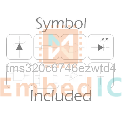
ECAD Model

Symbol

TMS320C6746EZWTD4

Footprint

TMS320C6746EZWTD4

Features

  • 375- and 456-MHz C674x Fixed- and Floating-Point VLIW DSP
  • C674x Instruction Set Features
    • Superset of the C67x+ and C64x+ ISAs
    • Up to 3648 MIPS and 2746 MFLOPS
    • Byte-Addressable (8-, 16-, 32-, and 64-Bit Data)
    • 8-Bit Overflow Protection
    • Bit-Field Extract, Set, Clear
    • Normalization, Saturation, Bit-Counting
    • Compact 16-Bit Instructions
  • C674x Two-Level Cache Memory Architecture
    • 32KB of L1P Program RAM/Cache
    • 32KB of L1D Data RAM/Cache
    • 256KB of L2 Unified Mapped RAM/Cache
    • Flexible RAM/Cache Partition (L1 and L2)
  • Enhanced Direct Memory Access Controller 3 (EDMA3):
    • 2 Channel Controllers
    • 3 Transfer Controllers
    • 64 Independent DMA Channels
    • 16 Quick DMA Channels
    • Programmable Transfer Burst Size
  • TMS320C674x Floating-Point VLIW DSP Core
    • Load-Store Architecture With Nonaligned Support
    • 64 General-Purpose Registers (32-Bit)
    • Six ALU (32- and 40-Bit) Functional Units
      • Supports 32-Bit Integer, SP (IEEE Single Precision/32-Bit) and DP (IEEE Double Precision/64-Bit) Floating Point
      • Supports up to Four SP Additions Per Clock, Four DP Additions Every Two Clocks
      • Supports up to Two Floating-Point (SP or DP) Reciprocal Approximation (RCPxP) and Square-Root Reciprocal Approximation (RSQRxP) Operations Per Cycle
    • Two Multiply Functional Units:
      • Mixed-Precision IEEE Floating-Point Multiply Supported up to:
        • 2 SP × SP → SP Per Clock
        • 2 SP × SP → DP Every Two Clocks
        • 2 SP × DP → DP Every Three Clocks
        • 2 DP × DP → DP Every Four Clocks
      • Fixed-Point Multiply Supports Two 32 × 32-Bit Multiplies, Four 16 × 16-Bit Multiplies, or Eight 8 × 8-Bit Multiplies per Clock Cycle, and Complex Multiples
    • Instruction Packing Reduces Code Size
    • All Instructions Conditional
    • Hardware Support for Modulo Loop Operation
    • Protected Mode Operation
    • Exceptions Support for Error Detection and Program Redirection
  • Software Support
    • TI DSPBIOS
    • Chip Support Library and DSP Library
  • 1.8-V or 3.3-V LVCMOS I/Os (Except for USB and DDR2 Interfaces)
  • Two External Memory Interfaces:
    • EMIFA
      • NOR (8- or 16-Bit-Wide Data)
      • NAND (8- or 16-Bit-Wide Data)
      • 16-Bit SDRAM With 128-MB Address Space
    • DDR2/Mobile DDR Memory Controller With one of the Following:
      • 16-Bit DDR2 SDRAM With 256-MB Address Space
      • 16-Bit mDDR SDRAM With 256-MB Address Space
  • Three Configurable 16550-Type UART Modules:
    • With Modem Control Signals
    • 16-Byte FIFO
    • 16x or 13x Oversampling Option
  • Two Serial Peripheral Interfaces (SPIs) Each With Multiple Chip Selects
  • Two Multimedia Card (MMC)/Secure Digital (SD) Card Interfaces With Secure Data I/O (SDIO) Interfaces
  • Two Master and Slave Inter-Integrated Circuits
    (I2C Bus)
  • One Host-Port Interface (HPI) With 16-Bit-Wide Muxed Address and Data Bus For High Bandwidth
  • Programmable Real-Time Unit Subsystem (PRUSS)
    • Two Independent Programmable Real-Time Unit (PRU) Cores
      • 32-Bit Load-Store RISC Architecture
      • 4KB of Instruction RAM Per Core
      • 512 Bytes of Data RAM Per Core
      • PRUSS can be Disabled Through Software to Save Power
      • Register 30 of Each PRU is Exported From the Subsystem in Addition to the Normal R31 Output of the PRU Cores.
    • Standard Power-Management Mechanism
      • Clock Gating
      • Entire Subsystem Under a Single PSC Clock Gating Domain
    • Dedicated Interrupt Controller
    • Dedicated Switched Central Resource
  • USB 2.0 OTG Port With Integrated PHY (USB0)
    • USB 2.0 High- and Full-Speed Client
    • USB 2.0 High-, Full-, and Low-Speed Host
    • End Point 0 (Control)
    • End Points 1, 2, 3, and 4 (Control, Bulk, Interrupt, or ISOC) RX and TX
  • One Multichannel Audio Serial Port (McASP):
    • Two Clock Zones and 16 Serial Data Pins
    • Supports TDM, I2S, and Similar Formats
    • DIT-Capable
    • FIFO Buffers for Transmit and Receive
  • Two Multichannel Buffered Serial Ports (McBSPs):
    • Supports TDM, I2S, and Similar Formats
    • AC97 Audio Codec Interface
    • Telecom Interfaces (ST-Bus, H100)
    • 128-Channel TDM
    • FIFO Buffers for Transmit and Receive
  • 10/100 Mbps Ethernet MAC (EMAC):
    • IEEE 802.3 Compliant
    • MII Media-Independent Interface
    • RMII Reduced Media-Independent Interface
    • Management Data I/O (MDIO) Module
  • Video Port Interface (VPIF):
    • Two 8-Bit SD (BT.656), Single 16-Bit or Single Raw (8-, 10-, and 12-Bit) Video Capture Channels
    • Two 8-Bit SD (BT.656), Single 16-Bit Video Display Channels
  • Universal Parallel Port (uPP):
    • High-Speed Parallel Interface to FPGAs and Data Converters
    • Data Width on Both Channels is 8- to 16-Bit Inclusive
    • Single-Data Rate or Dual-Data Rate Transfers
    • Supports Multiple Interfaces With START, ENABLE, and WAIT Controls
  • Real-Time Clock (RTC) With 32-kHz Oscillator and Separate Power Rail
  • Three 64-Bit General-Purpose Timers (Each Configurable as Two 32-Bit Timers)
  • One 64-Bit General-Purpose or Watchdog Timer (Configurable as Two 32-Bit General-Purpose Timers)
  • Two Enhanced High-Resolution Pulse Width Modulators (eHRPWMs):
    • Dedicated 16-Bit Time-Base Counter With Period and Frequency Control
    • 6 Single-Edge Outputs, 6 Dual-Edge Symmetric Outputs, or 3 Dual-Edge Asymmetric Outputs
    • Dead-Band Generation
    • PWM Chopping by High-Frequency Carrier
    • Trip Zone Input
  • Three 32-Bit Enhanced Capture (eCAP) Modules:
    • Configurable as 3 Capture Inputs or 3 Auxiliary Pulse Width Modulator (APWM) Outputs
    • Single-Shot Capture of up to Four Event Timestamps
  • Packages:
    • 361-Ball Pb-Free Plastic Ball Grid Array (PBGA) [ZCE Suffix], 0.65-mm Ball Pitch
    • 361-Ball Pb-Free PBGA [ZWT Suffix],
      0.80-mm Ball Pitch
  • Commercial, Extended, or Industrial Temperature

Applications

TMS320C674x

Specifications

  • Clock Rate 456MHz

  • Operating Temperature -40℃ ~ 90℃ (TJ)

  • Type Fixed/Floating Point

  • Non-Volatile Memory ROM (1.088 MB)

  • Package / Case 361-LFBGA

  • Voltage - Core 1.00V, 1.10V, 1.20V, 1.30V

  • Voltage - I/O 1.8V, 3.3V

  • Mounting Type Surface Mount

  • Interface EBI/EMI, Ethernet MAC, Host Interface, I2C, McASP, McBSP, SPI, UART, USB

  • Supplier Device Package 361-NFBGA (16x16)

  • On-Chip RAM 488kB

Circuit Diagram

Popular Products

  • FMS7401LEN14

    Manufacturer: ON Semiconductor

    IC CTRLR POWER DGTL EEPROM 14DIP

    Product Categories: MCU

    Lifecycle:

    RoHS:

  • Z8930012PSG

    Manufacturer: Zilog

    IC TV/VCR CTRL 24K OTP 40-DIP

    Product Categories: DSP

    Lifecycle:

    RoHS:

  • Z9024106PSG

    Manufacturer: Zilog

    IC 32K 8 BIT DTC OTP 42-DIP

    Product Categories: MCU

    Lifecycle:

    RoHS:

  • MB96F633ABPMC-GE1

    Manufacturer: Cypress

    IC MCU 16BIT 96KB FLASH 80LQFP

    Product Categories: 16bit MCU

    Lifecycle:

    RoHS:

  • SAF-XC164CM-16F20F BA

    Manufacturer: Infineon

    IC MCU 16BIT 128KB FLASH 64LQFP

    Product Categories: 16bit MCU

    Lifecycle:

    RoHS:

  • SAF-XC164D-32F40F BB

    Manufacturer: Infineon

    IC MCU 16BIT 256KB FLASH 100TQFP

    Product Categories: 16bit MCU

    Lifecycle:

    RoHS:

  • SAF-XC164GM-16F20F BA

    Manufacturer: Infineon

    IC MCU 16BIT 128KB FLASH 64LQFP

    Product Categories: 16bit MCU

    Lifecycle:

    RoHS:

  • ATAM862P-TNSY3D

    Manufacturer: Microchip

    IC MCU FLASH 4K TX 315MHZ 24SSOP

    Product Categories: MCU

    Lifecycle:

    RoHS:

  • CY7C63513C-PVXC

    Manufacturer: Cypress

    IC MCU 8K USB LS PERIPH 48SSOP

    Product Categories: General MCU

    Lifecycle:

    RoHS:

Product evaluation

  • Looking forward to your comment

  • Comment

    Verification Code * 

Compare products

Compare Empty