Hello! Welcome to Embedic!

Pictures are for reference only Please prevail in kind
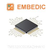
IC DSP FIXED-POINT 144BGA
 PCB Symbol, Footprint
 Send Inquiry
 Download Datasheet
 SUPPLIERS WHOLESALE PRICE TRENDS
Price comparison from authorized distributors
 TMS320C5535AZHHA10 Competitive Prices
EmbedIC has the unique source of supply. We can offer TMS320C5535AZHHA10 more competitive price for our customers. You can enjoy our best service by purchasing Texas Instruments TMS320C5535AZHHA10, Please feel free to contact for the best price of TMS320C5535AZHHA10 DSP. Click To Get Quotation
These devices are members of TI's C5000 fixed-point Digital Signal Processor (DSP) product family and are designed for low-power applications.
The fixed-point DSP is based on the TMS320C55x DSP generation CPU processor core. The C55x DSP architecture achieves high performance and low power through increased parallelism and total focus on power savings. The CPU supports an internal bus structure that is composed of one program bus, one 32-bit data read bus and two 16-bit data read buses, two 16-bit data write buses, and additional buses dedicated to peripheral and DMA activity. These buses provide the ability to perform up to four 16-bit data reads and two 16-bit data writes in a single cycle. The device also includes four DMA controllers, each with 4 channels, providing data movement for 16-independent channel contexts without CPU intervention. Each DMA controller can perform one 32-bit data transfer per cycle, in parallel and independent of the CPU activity.
The C55x CPU provides two multiply-accumulate (MAC) units, each capable of 17-bit x 17-bit multiplication and a 32-bit add in a single cycle. A central 40-bit arithmetic and logic unit (ALU) is supported by an additional 16-bit ALU. Use of the ALUs is under instruction set control, providing the ability to optimize parallel activity and power consumption. These resources are managed in the Address Unit (AU) and Data Unit (DU) of the C55x CPU.
The C55x CPU supports a variable byte width instruction set for improved code density. The Instruction Unit (IU) performs 32-bit program fetches from internal or external memory and queues instructions for the Program Unit (PU). The PU decodes the instructions, directs tasks to the AU and DU resources, and manages the fully protected pipeline. Predictive branching capability avoids pipeline flushes on execution of conditional instructions.
The general-purpose input and output functions, along with the 10-bit SAR ADC on the TMS320C5535, provide sufficient pins for status, interrupts, and bit I/O for LCD displays, keyboards, and media interfaces. Serial media is supported through two secure digital (SD) peripherals, four Inter-IC Sound (I2S Bus) modules, one serial port interface (SPI) with up to four chip selects, one I2C multimaster and slave interface, and a universal asynchronous receiver/transmitter (UART) interface.
Additional peripherals include: a high-speed Universal Serial Bus (USB 2.0) device mode only (not available on TMS320C5532), a real-time clock (RTC), three general-purpose timers with one configurable as a watchdog timer, and an analog phase-locked loop (APLL) clock generator.
In addition, the TMS320C5535 includes a tightly coupled FFT Hardware Accelerator. The tightly coupled FFT Hardware Accelerator supports 8- to 1024-point (in power of 2) real and complex-valued FFTs.
Furthermore, the device includes the following three integrated LDOs to power different sections of the device.
ANA_LDO (all devices) provides 1.3 V to the DSP PLL (VDDA_PLL), SAR, and power-management circuits (VDDA_ANA).
DSP_LDO (TMS320C5535 and 'C5534) provides 1.3 V or 1.05 V to the DSP core (CVDD), selectable on-the-fly by software as long as operating frequency ranges are observed. For lowest power operation, the programmer can shut down the internal DSP_LDO, cutting power to the DSP core (CVDD) while an external supply provides power to the RTC (CVDDRTC and DVDDRTC). The RTC alarm interrupt or the WAKEUP pin can re-enable the internal DSP_LDO and re-apply power to the DSP core. When DSP_LDO comes out of reset, it is enabled to 1.3 V for the bootloader to operate. For the 50-MHz devices, DSP_LDO must be programmed to 1.05 V to match the core voltage, CVDD, for proper operation after reset.
USB_LDO (TMS320C5535, 'C5534, and 'C5533) provides 1.3 V to the USB core digital (USB_VDD1P3) and PHY circuits (USB_VDDA1P3).
These devices are supported by the industry’s award-winning eXpressDSP, Code Composer Studio Integrated Development Environment (IDE), DSP/BIOS, Texas Instruments’ algorithm standard, and the industry’s largest third-party network. Code Composer Studio IDE features code generation tools including a C Compiler and Linker, RTDX, XDS100, XDS510, XDS560 emulation device drivers, and evaluation modules. The devices are also supported by the C55x DSP library which features more than 50 foundational software kernels (FIR filters, IIR filters, FFTs, and various math functions) as well as chip support libraries.
Clock Rate 100MHz
Operating Temperature -40℃ ~ 85℃ (TC)
Type Fixed Point
Non-Volatile Memory ROM (128 kB)
Package / Case 144-LFBGA
Voltage - Core 1.05V, 1.30V
Voltage - I/O 1.8V, 2.5V, 2.75V, 3.3V
Mounting Type Surface Mount
Interface I2C, I2S, LCD, MMC/SD, SPI, UART, USB
Supplier Device Package 144-BGA MICROSTAR (12x12)
On-Chip RAM 320kB
Manufacturer: Cypress
IC MCU 8K USB HUB 4 PORT 28-SOIC
Product Categories: General MCU
Lifecycle:
RoHS:
Manufacturer: Cypress
IC MCU USB PERIPH HI SPD 56VQFN
Product Categories: USB MCU
Lifecycle:
RoHS:
Manufacturer: Cypress
IC MCU 3K USB LS PERIPH 18-DIP
Product Categories: General MCU
Lifecycle:
RoHS:
Manufacturer: ON Semiconductor
IC CTRLR POWER DGTL EEPROM 8DIP
Product Categories: MCU
Lifecycle:
RoHS:
Manufacturer: Zilog
IC Z8 DIG TV CTRL OTP 42-SDIP
Product Categories: MCU
Lifecycle:
RoHS:
Manufacturer: Infineon
IC MCU 16BIT 256KB FLASH 144TQFP
Product Categories: 16bit MCU
Lifecycle:
RoHS:
Manufacturer: Infineon
IC MCU 16BIT 256KB FLASH 144TQFP
Product Categories: 16bit MCU
Lifecycle:
RoHS:
Manufacturer: Infineon
IC MCU 16BIT 256KB FLASH 100TQFP
Product Categories: 16bit MCU
Lifecycle:
RoHS:
Manufacturer: Cypress
IC MCU 16BIT 160KB FLASH 80LQFP
Product Categories: 16bit MCU
Lifecycle:
RoHS:
Manufacturer: Microchip
IC MCU FLASH 4K TX 315MHZ 24SSOP
Product Categories: MCU
Lifecycle:
RoHS:
Looking forward to your comment
Comment
 Popular Searches
8 Bit MCU, Flash, PIC16 Family PIC16F7XX Series Microcontrollers, 20 MHz, 7 KB, ...
EEPROM 2K 256 X 8 2.5V SERIAL EE IND
System-On-Modules - SOM RCM2200
32-bit Arm Cortex-A53 vision processor with ISP, powerful 3D GPU, dual APEX-2 v...
IC MCU 8BIT 60KB FLASH 44QFP
DSP 20MHZ 44QFP
1
2
3
4
5
6
Product updates, events, and resources in your inbox


Smart System

Traffic Management

Security

Consumer Electronics

Wireless Technology

Robot

Internet of Things

Industrial Control