Hello! Welcome to Embedic!
This website uses cookies. By using this site, you consent to the use of cookies. For more information, please take a look at our Privacy Policy.
Home > Embedded ICs > 32bit MCU > LPC4088FET180,551
NXP

LPC4088FET180,551

Pictures are for reference only Please prevail in kind
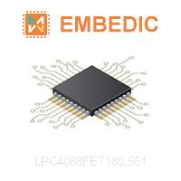
  • Quantity : *

  • Contact Name : *

  • Email : *

price SUPPLIERS WHOLESALE PRICE TRENDS

Price comparison from authorized distributors

price info LPC4088FET180,551 Competitive Prices

EmbedIC has the unique source of supply. We can offer LPC4088FET180,551 more competitive price for our customers. You can enjoy our best service by purchasing NXP LPC4088FET180,551, Please feel free to contact for the best price of LPC4088FET180,551 32bit MCU. Click To Get Quotation

LPC4088FET180,551 Overview

The LPC408x is an Arm Cortex-M4 based digital signal controller for embeddedapplications requiring a high level of integration and low power dissipation.

The Arm Cortex-M4 is a next generation core that offers system enhancements such aslow power consumption, enhanced debug features, and a high level of support blockintegration. The Arm Cortex-M4 CPU incorporates a 3-stage pipeline, uses a Harvardarchitecture with separate local instruction and data buses as well as a third bus forperipherals, and includes an internal prefetch unit that supports speculative branching.The Arm Cortex-M4 supports single-cycle digital signal processing and SIMDinstructions. A hardware floating-point processor is integrated in the core for severalversions of the part.

The LPC408x adds a specialized flash memory accelerator to accomplish optimalperformance when executing code from flash. The LPC408x is targeted to operate atup to 120 MHz CPU frequency.

The peripheral complement of the LPC408x includes up to 512 kB of flash programmemory, up to 96 kB of SRAM data memory, up to 4032 byte of EEPROM data memory,External Memory controller (EMC), LCD, Ethernet, USB Device/Host/OTG, an SPI FlashInterface (SPIFI), a General Purpose DMA controller, five UARTs, three SSP controllers,three I2C-bus interfaces, a Quadrature Encoder Interface, four general purpose timers,two general purpose PWMs with six outputs each and one motor control PWM, anultra-low power RTC with separate battery supply and event recorder, a windowedwatchdog timer, a CRC calculation engine and up to 165 general purpose I/O pins.

The analog peripherals include one eight-channel 12-bit ADC, two analog comparators,and a DAC.

The pinout of LPC408x is intended to allow pin function compatibility with theLPC24xx/23xx as well as the LPC178x/7x families.

Features

  • Functional replacement for LPC23xx/24xx and LPC178x family devices.
  • External Memory Controller (EMC) provides support for asynchronous static memory devices such as RAM, ROM and flash, as well as dynamic memories such as single data rate SDRAM.
  • Eight channel General Purpose DMA controller (GPDMA) on the AHB multilayer matrix that can be used with the SSP, I2S, UART, CRC engine, Analog-to-Digital and Digital-to-Analog converter peripherals, timer match signals, GPIO, and for memory-to-memory transfers.
  • Versatile pin function selection feature allows many possibilities for using on-chip peripheral functions.
  • Unique device serial number for identification purposes.
  • Single 3.3 V power supply (2.4 V to 3.6 V). Temperature range of -40 °C to 85 °C.
  • Available as LQFP208, TFBGA208, TFBGA180, LQFP144, and LQFP80 package.
Arm Cortex-M4 core
  • Arm Cortex-M4 processor, running at frequencies of up to 120 MHz.
  • Arm Cortex-M4 built-in Memory Protection Unit (MPU) supporting eight regions.
  • Arm Cortex-M4 built-in Nested Vectored Interrupt Controller (NVIC).
  • Hardware floating-point unit (not all versions).
  • Non-maskable Interrupt (NMI) input.
  • JTAG and Serial Wire Debug (SWD), serial trace, eight breakpoints, and four watch points.
  • System tick timer.
System
  • Multilayer AHB matrix interconnect provides a separate bus for each AHB master. AHB masters include the CPU, and General Purpose DMA controller. This interconnect provides communication with no arbitration delays unless two masters attempt to access the same slave at the same time.
  • Split APB bus allows for higher throughput with fewer stalls between the CPU and DMA. A single level of write buffering allows the CPU to continue without waiting for completion of APB writes if the APB was not already busy.
  • Embedded Trace Macrocell (ETM) module supports real-time trace.
  • Boundary scan for simplified board testing.
Memory
  • 512 kB on-chip flash program memory with In-System Programming (ISP) and In-Application Programming (IAP) capabilities. The combination of an enhanced flash memory accelerator and location of the flash memory on the CPU local code/data bus provides high code performance from flash.
  • Up to 96 kB on-chip SRAM includes: 64 kB of main SRAM on the CPU with local code/data bus for high-performance CPU access. Two 16 kB peripheral SRAM blocks with separate access paths for higher throughput. These SRAM blocks may be used for DMA memory as well as for general purpose instruction and data storage.
  • Up to 4032 byte on-chip EEPROM.
LCD controller, supporting both Super-Twisted Nematic (STN) and Thin-Film Transistors (TFT) displays
  • Dedicated DMA controller.
  • Selectable display resolution (up to 1024 x 768 pixels).
  • Supports up to 24-bit true-color mode.
Serial interfaces
  • Quad SPI Flash Interface (SPIFI) with four lanes and up to 40 MB per second.
  • Ethernet MAC with MII/RMII interface and associated DMA controller. These functions reside on an independent AHB.
  • USB 2.0 full-speed dual port device/host/OTG controller with on-chip PHY and associated DMA controller.
  • Five UARTs with fractional baud rate generation, internal FIFO, DMA support, and RS-485/EIA-485 support. One UART (UART1) has full modem control I/O, and one UART (USART4) supports IrDA, synchronous mode, and a smart card mode conforming to ISO7816-3.
  • Three SSP controllers with FIFO and multi-protocol capabilities. The SSP interfaces can be used with the GPDMA controller.
  • Three enhanced I²C-bus interfaces, one with a true open-drain output supporting the full I²C-bus specification and Fast-mode Plus with data rates of 1 Mbit/s, two with standard port pins. Enhancements include multiple address recognition and monitor mode.
  • I²S (Inter-IC Sound) interface for digital audio input or output. It can be used with the GPDMA.
  • CAN controller with two channels.
Digital peripherals
  • SD/MMC memory card interface.
  • Up to 165 General Purpose I/O (GPIO) pins depending on the packaging, with configurable pull-up/down resistors, open-drain mode, and repeater mode. All GPIOs are located on an AHB bus for fast access and support Cortex-M4 bit-banding. GPIOs can be accessed by the General Purpose DMA Controller. Any pin of ports 0 and 2 can be used to generate an interrupt.
  • Two external interrupt inputs configurable as edge/level sensitive. All pins on port 0 and port 2 can be used as edge sensitive interrupt sources.
  • Four general purpose timers/counters, with a total of eight capture inputs and ten compare outputs. Each timer block has an external count input. Specific timer events can be selected to generate DMA requests.
  • Quadrature encoder interface that can monitor one external quadrature encoder.
  • Two standard PWM/timer blocks with external count input option.
  • One motor control PWM with support for three-phase motor control.
  • Real-Time Clock (RTC) with a separate power domain. The RTC is clocked by a dedicated RTC oscillator. The RTC block includes 20 bytes of battery-powered backup registers, allowing system status to be stored when the rest of the chip is powered off. Battery power can be supplied from a standard 3 V lithium button cell. The RTC will continue working when the battery voltage drops to as low as 2.1 V. An RTC interrupt can wake up the CPU from any reduced power mode.
  • Event Recorder that can capture the clock value when an event occurs on any of three inputs. The event identification and the time it occurred are stored in registers. The Event Recorder is located in the RTC power domain and can therefore operate as long as there is RTC power.
  • Windowed Watchdog Timer (WWDT). Windowed operation, dedicated internal oscillator, watchdog warning interrupt, and safety features.
  • CRC Engine block can calculate a CRC on supplied data using one of three standard polynomials. The CRC engine can be used in conjunction with the DMA controller to generate a CRC without CPU involvement in the data transfer.
Analog peripherals
  • 12-bit Analog-to-Digital Converter (ADC) with input multiplexing among eight pins, conversion rates up to 400 kHz, and multiple result registers. The 12-bit ADC can be used with the GPDMA controller.
  • 10-bit Digital-to-Analog Converter (DAC) with dedicated conversion timer and DMA support.
  • Two analog comparators.
Power control
  • Four reduced power modes: Sleep, Deep-sleep, Power-down, and Deep power-down.
  • The Wake-up Interrupt Controller (WIC) allows the CPU to automatically wake up from any priority interrupt that can occur while the clocks are stopped in Deep-sleep, Power-down, and Deep power-down modes.
  • Processor wake-up from Power-down mode via any interrupt able to operate during Power-down mode (includes external interrupts, RTC interrupt, PORT0/2 pin interrupt, and NMI).
  • Brownout detect with separate threshold for interrupt and forced reset.
  • On-chip Power-On Reset (POR).
Clock generation
  • Clock output function that can reflect the main oscillator clock, IRC clock, RTC clock, CPU clock, USB clock, or the watchdog timer clock.
  • On-chip crystal oscillator with an operating range of 1 MHz to 25 MHz.
  • 12 MHz Internal RC oscillator (IRC) trimmed to 1% accuracy that can optionally be used as a system clock.
  • An on-chip PLL allows CPU operation up to the maximum CPU rate without the need for a high-frequency crystal. May be run from the main oscillator or the internal RC oscillator.
  • A second, dedicated PLL may be used for USB interface in order to allow added flexibility for the Main PLL settings.
Target Applications
  • Communications:
    • Point-of-sale terminals, web servers, multi-protocol bridges
  • Industrial/Medical:
    • Automation controllers, application control, robotics control, HVAC, PLC, inverters, circuit breakers, medical scanning, security monitoring, motor drive, video intercom
  • Consumer/Appliance:
    • Audio, MP3 decoders, alarm systems, displays, printers, scanners, small appliances, fitness equipment
  • Automotive:
    • After-market, car alarms, GPS/fleet monitors

Applications

LPC40xx

Specifications

  • Core Processor ARM Cortex M4

  • Speed 120MHz

  • Operating Temperature -40℃ ~ 85℃ (TA)

  • Program Memory Type FLASH

  • RAM Size 96K x 8

  • Peripherals Brown-out Detect/Reset, DMA, I2S, LCD, POR, PWM, WDT

  • Mounting Type Surface Mount

  • Oscillator Type Internal

  • Supplier Device Package 180-TFBGA (12x12)

  • EEPROM Size 4032 x 8

  • Package / Case 180-TFBGA

  • Core Size 32-Bit

  • Connectivity CANbus, EBI/EMI, Ethernet, I2C, IrDA, Microwire, QEI, SD, SPI, SSI, SSP, UART/USART, USB, USB OTG

  • Program Memory Size 512KB (512K x 8)

  • Data Converters A/D 8x12b; D/A 1x10b

  • Voltage - Supply (Vcc/Vdd) 2.4V ~ 3.6V

Popular Products

  • PIC12LF1822T-I/SN

    Manufacturer: Microchip

    IC MCU 8BIT 3.5KB FLASH 8SOIC

    Product Categories: 8bit MCU

    Lifecycle:

    RoHS:

  • CY90922NCSPMC-GS-237E1-ND

    Manufacturer: Cypress

    IC MCU 16BIT 256KB MROM 120LQFP

    Product Categories: 16bit MCU

    Lifecycle:

    RoHS:

  • R5F1007ADNA#W0

    Manufacturer: Renesas

    IC MCU 16BIT 16KB FLASH 24HWQFN

    Product Categories: 16bit MCU

    Lifecycle:

    RoHS:

  • TMS320F2806PZQ

    Manufacturer: Texas Instruments

    IC MCU 32BIT 64KB FLASH 100LQFP

    Product Categories: 32bit MCU

    Lifecycle:

    RoHS:

  • R5F64179LPFB#UC

    Manufacturer: Renesas

    IC MCU SMD

    Product Categories: General MCU

    Lifecycle:

    RoHS:

  • MPC8272CVRMIBA

    Manufacturer: NXP

    IC MPU MPC82XX 266MHZ 516BGA

    Product Categories: MPU

    Lifecycle:

    RoHS:

  • EFM8LB10F16E-B-QFN24

    Manufacturer: Silicon Labs

    IC MCU 8BIT 16KB FLASH 24QFN

    Product Categories: 8bit MCU

    Lifecycle:

    RoHS:

  • PIC18F43K22-E/P

    Manufacturer: Microchip

    IC MCU 8BIT 8KB FLASH 40DIP

    Product Categories: 8bit MCU

    Lifecycle:

    RoHS:

Product evaluation

  • Looking forward to your comment

  • Comment

    Verification Code * 

Compare products

Compare Empty