Hello! Welcome to Embedic!

Pictures are for reference only Please prevail in kind
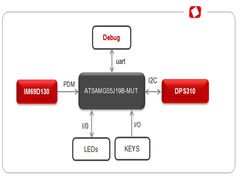
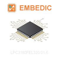
IC MCU 16/32BIT ROMLESS 320LFBGA
 PCB Symbol, Footprint
 Send Inquiry
 Download Datasheet
 SUPPLIERS WHOLESALE PRICE TRENDS
Price comparison from authorized distributors
 LPC3180FEL320/01,5 Competitive Prices
EmbedIC has the unique source of supply. We can offer LPC3180FEL320/01,5 more competitive price for our customers. You can enjoy our best service by purchasing NXP LPC3180FEL320/01,5, Please feel free to contact for the best price of LPC3180FEL320/01,5 32bit MCU. Click To Get Quotation
The LPC3180 is an ARM9-based microcontroller for embedded applications requiring high performance combined with low power dissipation. It achieves these objectives through the combination of NXP®'s state-of-the-art 90 nanometer technology with an ARM926EJ-S CPU core with a Vector Floating Point (VFP) coprocessor and a large array of standard peripherals including USB On-The-Go.
The microcontroller can operate at over 200 MHz CPU frequency (about 220 MIPS per Arm Inc.). The ARM926EJ-S CPU incorporates a 5-stage pipeline and has a Harvard architecture with separate 32 kB instruction and data caches, a demand paged MMU, DSP instruction extensions with a single cycle MAC, and Jazelle Java bytecode execution hardware. A block diagram of the microcontroller is shown .
Power optimization in this microcontroller is done through process and technology development (Intrinsic Power), and architectural means (Managed Power).
The LPC3180 also incorporates an SDRAM interface, NAND flash interfaces, USB 2.0 full-speed interface, seven UARTs, two I²C-bus interfaces, two SPI ports, a Secure Digital (SD) interface, and a 10-bit ADC in addition to many other features.
Core Processor ARM9?
Speed 208MHz
Operating Temperature -40℃ ~ 85℃ (TA)
Program Memory Type ROMless
RAM Size 64K x 8
Number of I/O 55
Peripherals DMA, PWM, WDT
Mounting Type Surface Mount
Oscillator Type External
Supplier Device Package 320-LFBGA (13x13)
Package / Case 320-LFBGA
Core Size 16/32-Bit
Connectivity EBI/EMI, I2C, Memory Card, SPI, UART/USART, USB OTG
Data Converters A/D 3x10b
Voltage - Supply (Vcc/Vdd) 1.1V ~ 3.3V
Manufacturer: STMicroelectronics
IC MCU 32BIT 256KB FLASH 100LQFP
Product Categories: 32bit MCU
Lifecycle:
RoHS:
Manufacturer: Intel
IC SOC CORTEX-A9 1.5GHZ 1152FBGA
Product Categories: SOC
Lifecycle:
RoHS:
Manufacturer: NXP
IC MCU 16BIT 256KB FLASH 112LQFP
Product Categories: 16bit MCU
Lifecycle:
RoHS:
Manufacturer: Silicon Labs
IC MCU 8BIT 32KB FLASH 32LQFP
Product Categories: 8bit MCU
Lifecycle:
RoHS:
Manufacturer: Microchip
IC MCU 8BIT 64KB FLASH 48UQFN
Product Categories: 8bit MCU
Lifecycle:
RoHS:
Manufacturer: Microchip
IC MCU 8BIT 96KB FLASH 80TQFP
Product Categories: 8bit MCU
Lifecycle:
RoHS:
Manufacturer: Infineon
IC MCU 16BIT 128KB FLASH 144TQFP
Product Categories: 16bit MCU
Lifecycle:
RoHS:
Manufacturer: NXP
IC MCU 8BIT 64KB FLASH 48LQFP
Product Categories: 8bit MCU
Lifecycle:
RoHS:
Manufacturer: Microchip
IC MCU 8BIT 14KB FLASH 44QFN
Product Categories: 8bit MCU
Lifecycle:
RoHS:
Looking forward to your comment
Comment
 Popular Searches
8 Bit MCU, Flash, PIC16 Family PIC16F7XX Series Microcontrollers, 20 MHz, 7 KB, ...
EEPROM 2K 256 X 8 2.5V SERIAL EE IND
System-On-Modules - SOM RCM2200
32-bit Arm Cortex-A53 vision processor with ISP, powerful 3D GPU, dual APEX-2 v...
IC MCU 8BIT 60KB FLASH 44QFP
DSP 20MHZ 44QFP
1
2
3
4
5
6
Product updates, events, and resources in your inbox


Smart System

Traffic Management

Security

Consumer Electronics

Wireless Technology

Robot

Internet of Things

Industrial Control