Hello! Welcome to Embedic!
This website uses cookies. By using this site, you consent to the use of cookies. For more information, please take a look at our Privacy Policy.
Home > Embedded ICs > 32bit MCU > LPC18S50FET180E
NXP

LPC18S50FET180E

Pictures are for reference only Please prevail in kind
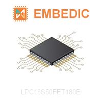
  • Quantity : *

  • Contact Name : *

  • Email : *

price SUPPLIERS WHOLESALE PRICE TRENDS

Price comparison from authorized distributors

price info LPC18S50FET180E Competitive Prices

EmbedIC has the unique source of supply. We can offer LPC18S50FET180E more competitive price for our customers. You can enjoy our best service by purchasing NXP LPC18S50FET180E, Please feel free to contact for the best price of LPC18S50FET180E 32bit MCU. Click To Get Quotation

LPC18S50FET180E Overview

The LPC18S50FET180 is a Arm Cortex-M3 based microcontroller with securityfeatures for embedded applications. The Arm Cortex-M3 is a next generation core thatoffers system enhancements such as low power consumption, enhanced debug features,and a high level of support block integration.

The LPC18S50FET180 operates at CPU frequencies of up to 180 MHz. The Arm Cortex-M3 CPU incorporates a 3-stage pipeline and uses a Harvard architecture withseparate local instruction and data buses as well as a third bus for peripherals. The Arm Cortex-M3 CPU also includes an internal prefetch unit that supports speculativebranching.

The LPC18S50FET180 includes 200 kB of on-chip SRAM, security features withAES engine, a quad SPI Flash Interface (SPIFI), a State Configurable Timer/PWM(SCTimer/PWM) subsystem, two High-speed USB controllers, Ethernet, LCD, an externalmemory controller, and multiple digital and analog peripherals.

Features

  • Processor core
    • Arm Cortex-M3 processor, running at frequencies of up to 180 MHz.
    • Arm Cortex-M3 built-in Memory Protection Unit (MPU) supporting eight regions.
    • Arm Cortex-M3 built-in Nested Vectored Interrupt Controller (NVIC).
    • Non-maskable Interrupt (NMI) input.
    • JTAG and Serial Wire Debug, serial trace, eight breakpoints, and four watch points.
    • Enhanced Trace Module (ETM) and Enhanced Trace Buffer (ETB) support.
    • System tick timer.
  • On-chip memory
    • 200 kB SRAM for code and data use.
    • Multiple SRAM blocks with separate bus access.
    • 64 kB ROM containing boot code and on-chip software drivers.
    • 64 bit One-Time Programmable (OTP) memory for general-purpose use.
    • Two banks (256 bit total) One-Time Programmable (OTP) memory for AES keystorage One bank can store an encrypted key for decoding the boot image.
  • AES engine for encryption and decryption of the boot image and data with DMAsupport and programmable via a ROM-based API.
  • Clock generation unit
    • Crystal oscillator with an operating range of 1 MHz to 25 MHz.
    • 12 MHz internal RC oscillator trimmed to 1.5 % accuracy over temperature andvoltage.
    • Ultra-low power RTC crystal oscillator.
    • Three PLLs allow CPU operation up to the maximum CPU rate without the need fora high-frequency crystal. The second PLL is dedicated to the High-speed USB, thethird PLL can be used as audio PLL.
    • Clock output.
  • Configurable digital peripherals:
    • State Configurable Timer (SCTimer/PWM) subsystem on AHB.
    • Global Input Multiplexer Array (GIMA) allows to cross-connect multiple inputs andoutputs to event driven peripherals like timers, SCTimer/PWM, and ADC0/1.
  • Serial interfaces
    • Quad SPI Flash Interface (SPIFI) with 1-, 2-, or 4-bit data at rates of up to52 MB per second.
    • 10/100T Ethernet MAC with RMII and MII interfaces and DMA support for highthroughput at low CPU load. Support for IEEE 1588 time stamping/advanced timestamping (IEEE 1588-2008 v2).
    • One High-speed USB 2.0 Host/Device/OTG interface with DMA support andon-chip high-speed PHY (USB0).
    • One High-speed USB 2.0 Host/Device interface with DMA support, on-chipfull-speed PHY and ULPI interface to an external high-speed PHY (USB1).
    • USB interface electrical test software included in ROM USB stack.
    • Four 550 UARTs with DMA support: one UART with full modem interface; oneUART with IrDA interface; three USARTs support UART synchronous mode and asmart card interface conforming to ISO7816 specification.
    • Up to two C_CAN 2.0B controllers with one channel each. Use of C_CAN controllerexcludes operation of all other peripherals connected to the same bus bridge.
    • Two SSP controllers with FIFO and multi-protocol support. Both SSPs with DMAsupport.
    • One Fast-mode Plus I2C-bus interface with monitor mode and with open-drain I/Opins conforming to the full I2C-bus specification. Supports data rates of up to1 Mbit/s.
    • One standard I²C-bus interface with monitor mode and standard I/O pins.
    • Two I²S interfaces with DMA support, each with one input and one output.
  • Digital peripherals
    • External Memory Controller (EMC) supporting external SRAM, ROM, NOR flash,and SDRAM devices.
    • LCD controller with DMA support and a programmable display resolution of up to1024 H x 768 V. Supports monochrome and color STN panels and TFT colorpanels; supports 1/2/4/8 bpp Color Look-Up Table (CLUT) and 16/24-bit direct pixelmapping.
    • Secure Digital Input Output (SD/MMC) card interface.
    • Eight-channel General-Purpose DMA controller can access all memories on theAHB and all DMA-capable AHB slaves.
    • Up to 118 General-Purpose Input/Output (GPIO) pins with configurablepull-up/pull-down resistors.
    • GPIO registers are located on the AHB for fast access. GPIO ports have DMAsupport.
    • Up to eight GPIO pins can be selected from all GPIO pins as edge and levelsensitive interrupt sources.
    • Two GPIO group interrupt modules enable an interrupt based on a programmablepattern of input states of a group of GPIO pins.
    • Four general-purpose timer/counters with capture and match capabilities.
    • One motor control PWM for three-phase motor control.
    • One Quadrature Encoder Interface (QEI).
    • Repetitive Interrupt timer (RI timer).
    • Windowed watchdog timer.
    • Ultra-low power Real-Time Clock (RTC) on separate power domain with 256 bytesof battery powered backup registers.
    • Alarm timer; can be battery powered.
  • Analog peripherals
    • One 10-bit DAC with DMA support and a data conversion rate of 400 kSamples/s.
    • Two 10-bit ADCs with DMA support and a data conversion rate of 400 kSamples/s.Up to eight input channels per ADC.
  • Unique ID for each device.
  • Power
    • Single 3.3 V (2.2 V to 3.6 V) power supply with on-chip internal voltage regulator forthe core supply and the RTC power domain.
    • RTC power domain can be powered separately by a 3 V battery supply.
    • Four reduced power modes: Sleep, Deep-sleep, Power-down, and Deeppower-down.
    • Processor wake-up from Sleep mode via wake-up interrupts from variousperipherals.
    • Wake-up from Deep-sleep, Power-down, and Deep power-down modes viaexternal interrupts and interrupts generated by battery powered blocks in the RTCpower domain.
    • Brownout detect with four separate thresholds for interrupt and forced reset.
    • Power-On Reset (POR).
  • Available as TFBGA180 package.
Target Applications
  • Communication hubs
  • Automotive aftermarket
  • Power management
  • Consumer health devices
  • Embedded audio applications
  • Industrial control
  • Industrial automation
  • White goods

Applications

LPC18xx

Specifications

  • Core Processor ARM Cortex M3

  • Speed 180MHz

  • Operating Temperature -40℃ ~ 85℃ (TA)

  • Program Memory Type ROMless

  • RAM Size 200K x 8

  • Number of I/O 118

  • Peripherals Brown-out Detect/Reset, DMA, I2S, LCD, POR, PWM, WDT

  • Mounting Type Surface Mount

  • Oscillator Type Internal

  • Supplier Device Package 180-TFBGA (12x12)

  • Package / Case 180-TFBGA

  • Core Size 32-Bit

  • Connectivity CANbus, EBI/EMI, Ethernet, I2C, IrDA, Microwire, QEI, MMC/SD, SPI, SSI, SSP, UART/USART, USB

  • Data Converters A/D 8x10b; D/A 1x10b

  • Voltage - Supply (Vcc/Vdd) 2.2V ~ 3.6V

Popular Products

  • 10AS066K3F40I2LG

    Manufacturer: Intel

    IC SOC CORTEX-A9 1.5GHZ 1517FBGA

    Product Categories: SOC

    Lifecycle:

    RoHS:

  • R5F51136ADLJ#20

    Manufacturer: Renesas

    IC MCU 32BIT 256KB FLASH 100LGA

    Product Categories: 32bit MCU

    Lifecycle:

    RoHS:

  • ATTINY4313-MUR

    Manufacturer: Microchip

    IC MCU 8BIT 4KB FLASH 20QFN

    Product Categories: 8bit MCU

    Lifecycle:

    RoHS:

  • PIC18F2523T-I/ML

    Manufacturer: Microchip

    IC MCU 8BIT 32KB FLASH 28QFN

    Product Categories: 8bit MCU

    Lifecycle:

    RoHS:

  • IA186ESPQF100IR03

    Manufacturer: Analog Devices

    IC MCU 8/16BIT ROMLESS 100QFP

    Product Categories: 16bit MCU

    Lifecycle:

    RoHS:

  • LM3S2911-EQC50-A2T

    Manufacturer: Texas Instruments

    IC MCU 32BIT 256KB FLASH 100LQFP

    Product Categories: 32bit MCU

    Lifecycle:

    RoHS:

  • LM3S2918-EQC50-A2T

    Manufacturer: Texas Instruments

    IC MCU 32BIT 256KB FLASH 100LQFP

    Product Categories: 32bit MCU

    Lifecycle:

    RoHS:

  • 10AS066N3F40I2LG

    Manufacturer: Intel

    IC SOC CORTEX-A9 1.5GHZ 1517FBGA

    Product Categories: SOC

    Lifecycle:

    RoHS:

  • MSP430FR2311IPW16R

    Manufacturer: Texas Instruments

    IC MCU 16BIT 3.75KB FRAM 16TSSOP

    Product Categories: 16bit MCU

    Lifecycle:

    RoHS:

  • MSP430FE423IPMR

    Manufacturer: Texas Instruments

    IC MCU 16BIT 8KB FLASH 64LQFP

    Product Categories: 16bit MCU

    Lifecycle:

    RoHS:

Product evaluation

  • Looking forward to your comment

  • Comment

    Verification Code * 

Compare products

Compare Empty