Hello! Welcome to Embedic!


Pictures are for reference only Please prevail in kind
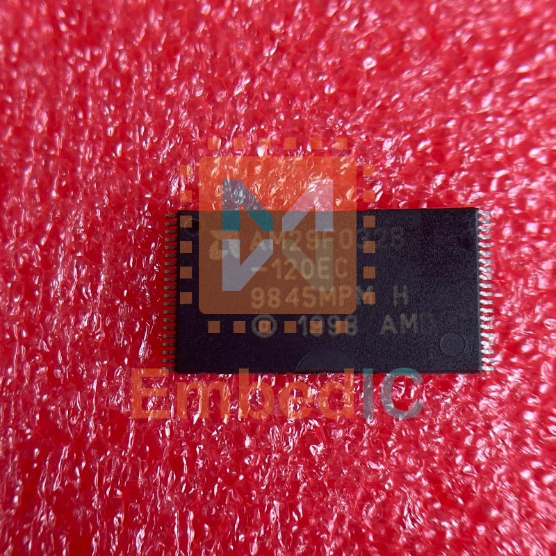
CONN PLUG .100 40POS DL PCB SMD
 PCB Symbol, Footprint
 Send Inquiry
 Download Datasheet
 SUPPLIERS WHOLESALE PRICE TRENDS
Price comparison from authorized distributors
 AM29F032B-120EC Competitive Prices
EmbedIC has the unique source of supply. We can offer AM29F032B-120EC more competitive price for our customers. You can enjoy our best service by purchasing AMD AM29F032B-120EC, Please feel free to contact for the best price of AM29F032B-120EC Controller. Click To Get Quotation
The Am29F032B is a 32 Mbit, 5.0 volt-only Flash memory organized as 4,194,304 bytes of 8 bits each. The 4 Mbytes of data are divided into 64 sectors of 64 Kbytes each for flexible erase capability. The 8 bits of data appear on DQ0–DQ7.
The Am29F032B is offered in 40-pin TSOP and 44-pin SO packages. The Am29F032B is manufactured using AMD’s 0.32 µm process technology. This device is designed to be programmed in-system with the standard system 5.0 volt VCC supply. A 12.0 volt VPP is not required for program or erase operations. The device can also be programmed in standard EPROM programmers.
The standard device offers access times of 70, 90, 120, and 150 ns, allowing high-speed microprocessors to operate without wait states. To eliminate bus contention, the device has separate chip enable (CE#), write enable (WE#), and output enable (OE#) controls.
The device is entirely command set compatible with the JEDEC single-power-supply Flash standard. Commands are written to the command register using standard microprocessor write timings. Register contents serve as input to an internal state machine that controls the erase and programming circuitry. Write cycles also internally latch addresses and data needed for the programming and erase operations. Reading data out of the device is similar to reading from 12.0 volt Flash or EPROM devices.
The device is programmed by executing the program command sequence. This invokes the Embedded Program algorithm—an internal algorithm that automatically times the program pulse widths and verifies proper cell margin. The device is erased by executing the erase command sequence. This invokes the Embedded Erase algorithm—an internal algorithm that automatically preprograms the array (if it is not already programmed) before executing the erase operation. During erase, the device automatically times the erase pulse widths and verifies proper cell margin.
The sector erase architecture allows memory sectors to be erased and reprogrammed without affecting the data contents of other sectors. A sector is typically erased and verified within one second. The device is erased when shipped from the factory.
The hardware sector group protection feature disables both program and erase operations in any combination of the eight sector groups of memory. A sector group consists of four adjacent sectors.
The Erase Suspend feature enables the system to put erase on hold for any period of time to read data from, or program data to, a sector that is not being erased. True background erase can thus be achieved.
The device requires only a single 5.0 volt power supply for both read and write functions. Internally generated and regulated voltages are provided for the program and erase operations. A low VCC detector automatically inhibits write operations during power transitions. The host system can detect whether a program or erase cycle is complete by using the RY/BY# pin, the DQ7 (Data# Polling) or DQ6 (toggle) status bits. After a program or erase cycle has been completed, the device automatically returns to the read mode.
A hardware RESET# pin terminates any operation in progress. The internal state machine is reset to the read mode. The RESET# pin may be tied to the system reset circuitry. Therefore, if a system reset occurs during either an Embedded Program or Embedded Erase algorithm, the device is automatically reset to the read mode. This enables the system’s microprocessor to read the boot-up firmware from the Flash memory.
AMD’s Flash technology combines years of Flash memory manufacturing experience to produce the highest levels of quality, reliability, and cost effectiveness. The device electrically erases all bits within a sector simultaneously via Fowler-Nordheim tunneling. The bytes are programmed one byte at a time using the programming mechanism of hot electron injection.
■ 5.0 V ± 10%, single power supply operation
— Minimizes system level power requirements
■ Manufactured on 0.32 µm process technology
■ High performance
— Access times as fast as 70 ns
■ Low power consumption
— 30 mA typical active read current
— 30 mA typical program/erase current
— <1 µA typical standby current (standard access time to active mode)
■ Flexible sector architecture
— 64 uniform sectors of 64 Kbytes each
— Any combination of sectors can be erased.
— Supports full chip erase
— Group sector protection:
— A hardware method of locking sector groups to prevent any program or erase operations within that sector group
— Temporary Sector Group Unprotect allows code changes in previously locked sectors
■ Embedded Algorithms
— Embedded Erase algorithm automatically preprograms and erases the entire chip or any combination of designated sectors
— Embedded Program algorithm automatically writes and verifies bytes at specified addresses
■ Minimum 1,000,000 write/erase cycles guaranteed
■ 20-year data retention at 125°C
— Reliable operation for the life of the system
■ Package options
— 40-pin TSOP
— 44-pin SO
■ Compatible with JEDEC standards
— Pinout and software compatible with single-power-supply Flash standard
— Superior inadvertent write protection
■ Data# Polling and toggle bits
— Provides a software method of detecting program or erase cycle completion
■ Ready/Busy output (RY/BY#)
— Provides a hardware method for detecting program or erase cycle completion
■ Erase Suspend/Resume
— Suspends a sector erase operation to read data from, or program data to, a non-erasing sector, then resumes the erase operation
■ Hardware reset pin (RESET#)
— Resets internal state machine to the read mode
Manufacturer: NXP
IC MCU 16BIT 256KB FLASH 112LQFP
Product Categories: 16bit MCU
Lifecycle:
RoHS:
Looking forward to your comment
Comment
 Popular Searches
8 Bit MCU, Flash, PIC16 Family PIC16F7XX Series Microcontrollers, 20 MHz, 7 KB, ...
EEPROM 2K 256 X 8 2.5V SERIAL EE IND
System-On-Modules - SOM RCM2200
32-bit Arm Cortex-A53 vision processor with ISP, powerful 3D GPU, dual APEX-2 v...
IC MCU 8BIT 60KB FLASH 44QFP
DSP 20MHZ 44QFP
1
2
3
4
5
6
Product updates, events, and resources in your inbox


Smart System

Traffic Management

Security

Consumer Electronics

Wireless Technology

Robot

Internet of Things

Industrial Control