Hello! Welcome to Embedic!
High efficiency and low THD dimmable LED 100W driver based on ST HVLED001B +HVLED002 design.
1. Introduction of HVLED001B:
HVLED001B is a high power factor flyback controller with constant voltage primary sensing and ultra-low standby power consumption. It is also an enhanced peak current mode controller that can mainly control high power factor (HPF) flyback or buck-boost. Primary-side regulation and optocoupler control can be applied independently on the chip, and can be achieved with precise regulation and very low standby power consumption under no-load conditions. The innovative ST high voltage technology allows HVLED001B to be directly connected to the input voltage, so that the device can be started and the input voltage can be monitored without external components. Effectively control abnormal conditions such as open circuit, output short circuit, input overvoltage or undervoltage, and circuit failures such as open loop and overcurrent of the main switch. The built-in intelligent automatic recovery timer (ART) function ensures automatic recovery of the application without any loss of reliability.
Its main features are: application in quasi-resonant (QR) topology, direct optocoupler connection, used for current loop adjustment with feedback disconnection detection, 800 V high voltage start, high power factor and low THD in the general range, Programmable frequency foldback, intelligent automatic reload timer (ART) to ensure a latch-free device, 0-10 compatible with PWM dimming.
Mainly used in: 1. Single-stage LED driver with high power factor; 2. Two-stage LED driver;
2. Introduction of HVLED002:
HVLED002 is a high-performance current-mode LED controller that provides the necessary functions to achieve offline or DC to DC fixed frequency current mode control schemes. The internally implemented circuit includes: a fine-tuning oscillator for precise duty cycle control, under-voltage lockout, a precision reference for fine-tuning the accuracy of the error amplifier input, a PWM comparator for current limit control, and source or drain The designed totem pole output stage has high peak current. The output stage suitable for driving N-channel MOSFETs is lower in the off state.
Its main features are: trimming the oscillator can achieve precise frequency control; the oscillator frequency can be guaranteed to be 250 kHz; the current mode works to 500 kHz; the latched PWM is used for cycle-by-cycle current limiting; internally adjusted reference voltage with Undervoltage lockout; high current totem pole output; hysteresis undervoltage lockout; low start-up and operating current.
3. Introduction of STEVAL-LLL008V1 demo board:
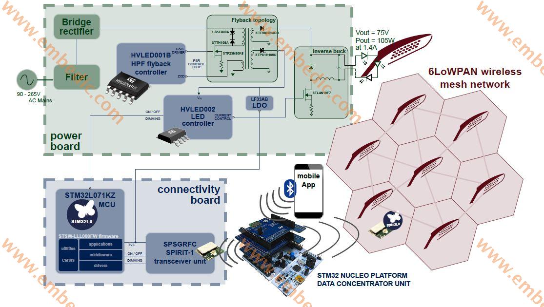
High-voltage LED street lights and area lighting applications usually require a rugged but efficient power supply to produce a tightly regulated output current with high power factor, low THD, and minimum voltage ripple. This design achieves very high efficiency through the HVLED001B controller, which drives the power MOSFET on the primary side of the STF23N80K5 AC/DC HPF flyback converter and regulates the voltage on the same primary side.
This reference design is a dual-stage LED driver with high power factor. It has very high power and is designed for 100 W LED lighting applications using 6LoWPAN mesh network. It contains two main parts, the power supply board and the connectivity daughter board.
Provide high power factor and low THD on the primary side flyback converter of the power main board, and realize CV primary side regulation through the input of the auxiliary winding of the transformer through the ZCD pin on the HVLED001B controller (manages the AC/DC HPF flyback converter) (PSR), so the main advantage of voltage loop primary side management is that no isolated optocoupler is required.
The flyback converter (J2 connector) can provide a reverse buck stage, which is driven by the HVLED002 controller through the STL4N10F7 power MOSFET, providing 105W of power, an average output voltage of 79V, and a maximum ripple of 1.8 V, can provide a stable 1.4A current to the LED driver load. The secondary transformer can also provide (a few milliamps through an auxiliary choke) the voltage required to power up the HVLED002 controller, which manages the current limit of the anti-buck circuit for dimming effects and on/off control.
Fourth, STM32L071KZ microcontroller
STEVAL-LLL008V1 integrates the STM32L071KZ microcontroller, which can receive remote on, off and dimming commands through the embedded SPSGRFC sub-1 GHz transceiver module. The connection function can be extended to multiple lighting nodes in the 6LowPAN mesh network. The daughter board can be connected through the J12-4 pin connector on the power board. Pin 1 uses 3.3 V to power the control board; Pin 4 provides common GND; Pin 3 is used to enable/disable the signal of the control board; Pin 2 is used for the PWM dimming signal from the control board.
Data Concentrator (DCU) and mobile Android applications have been developed to help you further explore the LED lighting reference design. DCU is composed of NUCLEO-F401RE development platform, X-NUCLEO-IDS01A4 for communication with LED driver board below 1 GHz and X-NUCLEO-IDB05A2 board for Bluetooth communication with mobile devices.
The ST 6LoWPAN smart street light mobile application collects lighting node descriptions through the microcontroller and RF module on the evaluation board in the 6LoWPAN mesh network.
The overall design provides high efficiency, PSR control loop without optocoupler, and options to connect the control board to a programmable STM32 microcontroller to achieve dimming and enable/disable functions.
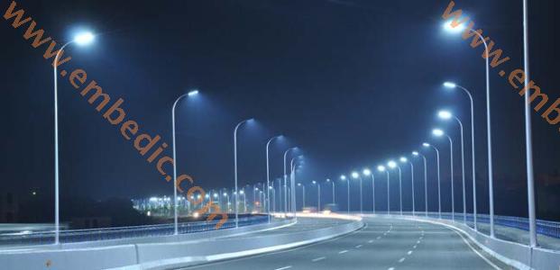
► Scenario application diagram
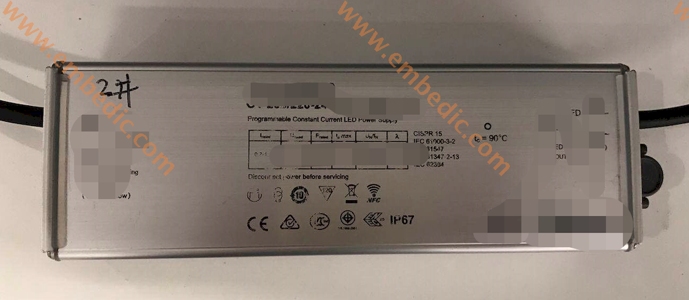
► Product entity diagram
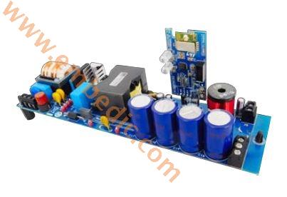
► Showcase photos
► Scheme block diagram
► Core technical advantages
► Solution specifications

IC MCU 8BIT 160KB FLASH 52LQFP

IC MCU 32BIT 64KB FLASH 64LQFP
IC MCU 16BIT 256KB FLASH 100TQFP

IC MCU 8BIT 1.5KB OTP 18SOIC
1
2
3
4
5
6


Product updates, events, and resources in your inbox


Smart System

Traffic Management

Security

Consumer Electronics

Wireless Technology

Robot

Internet of Things

Industrial Control