Hello! Welcome to Embedic!
The wireless transmission method collects, sends, and receives data, and processes the wirelessly collected data through the upper computer to control and monitor the operation of the equipment and reduce unnecessary line equipment expenses.
In today's industrial and agricultural production, there are more and more occasions for temperature and humidity collection, and accurate and convenient temperature measurement becomes crucial. Traditional wired temperature measurement methods have problems such as complicated wiring, easy aging of wiring, difficulty in troubleshooting, and re-wiring of equipment when re-layout. Especially in the case that the wired network is not smooth or the wiring is inconvenient to set up due to the limitation of the on-site environmental factors, it brings great trouble to the data collection of temperature and humidity. If you want to monitor real-time temperature and humidity data, you must use wireless transmission to collect, send, and receive data, and process the wirelessly collected data through the host computer to control and monitor the operation of the equipment and reduce unnecessary Line equipment expenses.
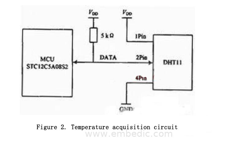
Design of temperature and humidity acquisition circuit
It is a temperature and humidity composite sensor with calibrated digital signal output. The sensor uses dedicated digital module acquisition technology and temperature and humidity sensing technology, with extremely high reliability and excellent long-term stability. Figure 2 shows its temperature acquisition circuit. The sensor includes a resistive humidity sensing element and an NTC temperature measuring element, which can be connected to a high-performance 8-bit microcontroller. The calibration coefficients are stored in the OTP memory in the form of programs, and these calibration coefficients can be called in the sensor during the signal detection process. The single-wire serial interface makes system integration simple and fast, and the signal transmission distance can reach more than 20m. When the length of the connecting wire is shorter than 20m, a 5kΩ pull-up resistor should be used. When it is longer than 20m, a suitable pull-up resistor should be used according to the situation.
Wireless transmitting and receiving circuit design
nRF24L01 is a wireless communication chip produced by NORDIC, which adopts FSK modulation method and integrates NORDIC's own Enhanced Short Burst protocol. It can realize point-to-point or 1-to-6 wireless communication. The wireless communication speed can reach 2 Mb/s. The circuit schematic diagram of the NORDIC wireless transmitting and receiving chip nRF24L01 is shown in Figure 3.
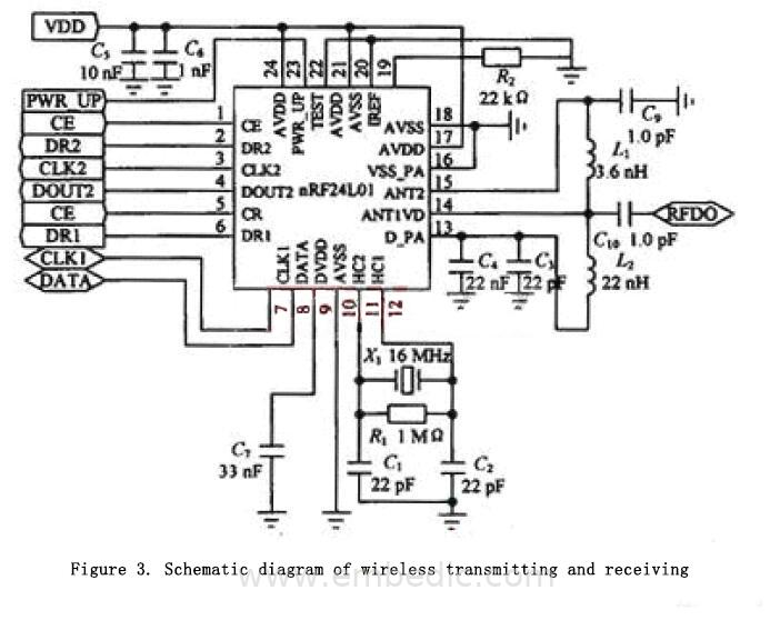
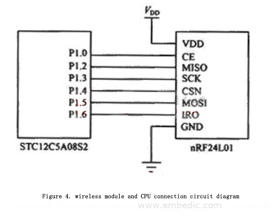
nRF24L01 is a single-chip radio frequency transceiver chip that works in the 2.4~2.5 GHz ISM frequency band. The chip has built-in functional modules such as frequency synthesizer, power amplifier, crystal oscillator, and modulator. The output power and communication channel can be configured through programs. The energy consumption of the nRF24L01 chip is very low. When transmitting with a power of -5 dBm, the working current is only 10.5 mA, and the working current when receiving is only 18 mA. It has a variety of low-power working modes, energy saving and environmental protection, and convenient design. The function of each pin of the nRF24L01 wireless transceiver module is listed in Table 1. Figure 4 shows the circuit diagram when nRF24L01 is connected to the microcontroller.
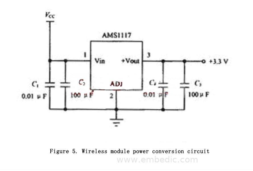
The power supply required by the wireless transmitting and receiving module is 1.9~3.6 V. In this system, a 3.3 V DC power supply is used to directly power the wireless transmitting and receiving module, and the 5 V power supply is used. After the ASM1117-3.3 chip is converted, a stable DC power supply can be obtained. The power conversion circuit is shown in Figure 5.
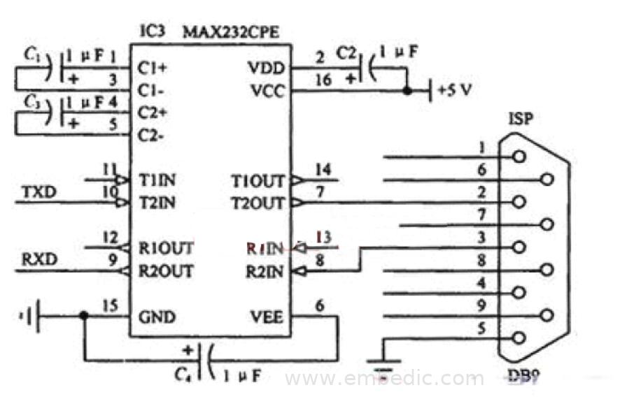
Serial communication module
After the host MCU receives the data of nRF24L01, the MCU program can be downloaded and upgraded by MAX232 level conversion. At the same time, it can realize the communication between the MCU and the PC (upper computer), so that the display data information can be transmitted to the PC through this circuit and coexist. Displayed on the PC, its serial communication circuit is shown in Figure 6.
This paper proposes a solution to the wireless data transmission problem, which is based on nRF24L01 to design a wireless temperature acquisition system. The system uses low-power, high-performance single-chip STC12C5A08S2 and temperature and humidity sensors to form a multi-point, real-time temperature and humidity monitoring system, and finally completes the configuration, display and alarm functions on the PC. The system is easy to use, easy to expand, and can be widely used in various industrial and agricultural production and breeding occasions.

IC MCU 8BIT 1KB FLASH 8DIP
IC MCU 16BIT 128KB FLASH 48TQFP
IC MCU 32BIT 256KB FLASH 64LFBGA
1
2
3
4
5
6


Product updates, events, and resources in your inbox


Smart System

Traffic Management

Security

Consumer Electronics

Wireless Technology

Robot

Internet of Things

Industrial Control