Hello! Welcome to Embedic!
Hello everyone, this is Erin. Welcome to the new post today. Today I will introduce everything about the memory controllers, including their classification of memory controllers, how it works, and the advantages and disadvantages of it. Let’s move on.
The memory controller is an important part of a computer system that controls the memory and is responsible for exchanging data between the memory and the CPU. It determines the memory performance of a computer system and thus has a large impact on the overall performance of the computer system.
With the growth of computer technology, memory controllers are split into 2 types: traditional type and integrated type.
The memory controller of the traditional computer system is set inside the north bridge chip of the motherboard chipset. To exchange data between the CPU and the memory, it needs to go through five steps of "CPU--North Bridge--Memory--North Bridge--CPU". Multi-level transmission, the data delay is undoubtedly relatively huge, which impacts the total efficiency of the computer system.
The integrated memory controller is a built-in memory controller on the CPU substrate. So how the system works without a memory controller?
26 data A~Z are to be sent to the CPU. Currently, the CPU sends an instruction to the north bridge (since the memory controller is integrated on the north bridge, so as it states that it pass through the north bridge), and the memory gets the instruction with the memory controller. This instruction is The A~Z data of unit b on the memory is transferred to the CPU, and the memory starts to fetch data at this time, which is commonly referred to as addressing.
Through evaluation, it is thought that it only takes one second to transfer to the CPU. Right now, the data is only transmitted to the north bridge in one second. The memory controller is in the north bridge. How to transmit the data in the north bridge to the CPU? This is through the FSB. Front side bus, assuming that the frequency of FSB is 800MHZ, then the data transfer rate is 800MHZ multiplied by 64BIT divided by 8 bits per second = 6.4GB per second, and it takes 2 seconds from the north bridge to the CPU, so the total time for data transmission to the CPU is 3 seconds, let's take a look at how the system works when the CPU integrates the memory controller;
After the data is transferred from the memory to the controller, it is also 1 second, the difference is that this time there is no need to go through the slow front-side bus, the CPU can directly read the data from the memory controller, and the CPU of the integrated memory controller reads the data. It only took 1 second to fetch 12GB of data, so the computing time was greatly saved, and the performance of the CPU was fully utilized.
Finally, to summarize: when the CPU does not have a memory controller, the data is transmitted in the way of the memory controller---North Bridge---CPU; when there is a memory controller, the data is transmitted in the way of the memory controller---CPU, complete in one step.
Like the CPU, the memory also has its own operating frequency. The frequency is measured in MHz. The greater the main frequency of the memory, to a particular degree, the faster the memory can achieve. The primary regularity of the memory identifies the maximum regularity at which the memory can work generally. The most mainstream memory types are DDR3 as well as DDR4. As an alternative to DDR2, the frequency of DDR3 memory has reached 1600MHz, while the frequency of DDR4 memory is 2133MHz.Memory Capacity.
The capacity of memory is not only a factor that affects the price of memory, but also a factor that affects the performance of the whole system. In the past, on the Windows XP platform, 512M of memory was still the mainstream, and 1GB was already a large capacity; 64-bit systems became popular, and more and more people used Windows Vista, Windows 7, and Windows 10. Without about 2GB of memory, smooth operation may not be guaranteed. Spend. The capacity of a single root memory is mainly 1GB, 2GB, 4GB, and the highest has reached a single root of 8GB and a single root of 16GB.
The voltage value required for the normal operation of the memory is different for different types of memory, but each has its own specifications.
Exceeding its specifications can easily cause damage to the memory. The functioning voltage of DDR2 memory is usually around 1.8V, and the DDR3 memory is around 1.5V or 1.35V. In order to overclock, the memory needs to work at a higher voltage value than the standard. So for each brand and model of memory, it depends on the manufacturer of them.
As long as it floats within the allowable range, slightly increasing the memory voltage is beneficial for memory overclocking, but at the same time, the heat generation is greatly increased, so there is a danger of damaging the hardware.
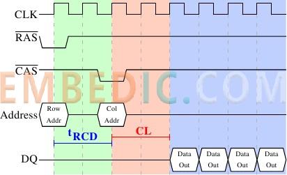
tCL : CAS Latency Control(tCL)
Generally, when we look up the timing parameters of the memory, such as digital sequences such as "8-8-8-24", the parameters corresponding to the above digital sequences are "CL-tRCD-tRP-tRAS". The first "8" is the first parameter, "CL".
CAS Latency Control (refered to tCL, CL, CAS Latency Time, CAS Timing Delay), it is "the latency of the front-line address controller for memory read and write operations". CAS controls the time between when an instruction is accepted and when it is executed. Due to the fact that CAS mainly regulates the hexadecimal address, or the column address in the memory matrix, it is one of the most vital parameter and also needs to be established as low as feasible under the premise of security.
This parameter has the greatest impact on memory performance. On the premise of ensuring system stability, the lower the CAS value, the faster the memory read and write operations.
tRCD : RAS to CAS Delay
This worth is the 2nd parameter in the "8-8-8-24" memory timing specifications, that is, the second "8". RAS to CAS Hold-up (also described as: tRCD, RAS to CAS Hold-up, Active to CMD), means "row addressing to column addressing delay time", the smaller the worth, the much better the efficiency.
When reading, writing, or refreshing the memory, a delay clock cycle needs to be inserted between the two pulse signals. In the JEDEC requirements, it is the second criterion, minimizing this hold-up can enhance system performance. If your memory does not overclock well, you can set this value to the memory's default value or try increasing the tRCD value.
tRP : Row Precharge Timing(tRP)
In the "8-8-8-24" memory timing parameters, the value is the third parameterthat "8". Row Precharge Timing shows "memory row address controller precharge time", so the smaller sized the precharge parameter, the quicker the memory read as well as also write speed. tRP is used to set the time required to charge the RAS before another row can be activated.
tRAS : Min RAS Active Timing
The value of last parameter in the "8-8-8-24" memory timing parameters is "24". Minutes RAS Active Time (also referred to as: tRAS, Energetic to Precharge Hold-up, Row Energetic Time, Precharge Wait State, Row Active Delay, Row Precharge Delay, RAS Energetic Time), indicates "the quickest period from memory row valid to precharge" , Adjusting this parameter needs to be determined according to the specific situation, generally we'd better set it between 24 and 30. This parameter depends on the actual situation, it does not mean that bigger or smaller is better.
If the period of tRAS is too long, the system will degrade performance due to unnecessary waiting. Decreasing the tRAS period will cause the activated row addresses to enter the deactivated state earlier. If the period of tRAS is too short, there may not be enough time to complete the burst transfer of data, which may result in lost or corrupted data. This value is generally set to CAS latency + tRCD + 2 clock cycles.
1. It can effectively control the memory controller to work at the same frequency as the CPU core, and because the data exchange between the memory and the CPU does not need to undergo the north bridge, it can efficiently decrease the transmission hold-up.
2. Decrease the worry of the North Bridge chip. Since the data exchange between CPU and memory accounts for a large proportion of the entire computer data exchange, the workload of the North Bridge chip is greatly reduced after integration, which can be used for SATA, PCI-E, etc. Data exchange channels provide more efficient support.
The adaptability to memory is relatively poor, and the flexibility is relatively poor. Only specific types of memory can be used, and there are restrictions on the capacity and speed of memory. To support new types of memory, the memory controller integrated inside the CPU must be updated. That is to say, a new CPU must be replaced;
For example, AMD's K8 series CPU can only support DDR, but cannot support higher-speed DDR2. However, the memory controller of the traditional solution does not have this problem because it is located inside the north bridge chip of the motherboard chipset. It is only necessary to replace the motherboard, or even without replacing the motherboard, different types of memory can be used, such as Intel Pentium4 series CPU, if the original configuration If the motherboard does not support DDR2, you can use DDR2 only by replacing a motherboard that supports DDR2. If it is equipped with a motherboard that supports both DDR and DDR2, you can use DDR2 directly without replacing the motherboard.
In the typical computer system, the memory controller lies inside the north bridge chip of the motherboard chipset. To exchange data between the CPU and the memory, it needs to go through five steps of "CPU--North Bridge--Memory--North Bridge--CPU", in this mode Data is transmitted through multiple stages, as well as the data hold-up is obviously relatively big, which impacts the overall efficiency of the computer system.
AMD's K8 series CPU (including various processors with interfaces such as Socket 754/939/940) integrates a memory controller, and the data exchange process between CPU and memory is simplified as "CPU--memory--CPU" "3 actions, leaving out 2 actions, clearly has lower information latency compared to the standard memory controller scheme, which aids to enhance the total performance of the computer system.

Manufacturer: Texas Instruments
IC DSP FIX/FLOAT POINT 361NFBGA
Product Categories: DSP
Lifecycle:
RoHS:
Manufacturer: Texas Instruments
IC DSP FIX/FLOAT POINT 361NFBGA
Product Categories: DSP
Lifecycle:
RoHS:
Manufacturer: Texas Instruments
IC DGTL MEDIA SOC 337NFBGA
Product Categories: SOC
Lifecycle:
RoHS:
Manufacturer: Texas Instruments
IC DGTL MEDIA SOC 337NFBGA
Product Categories: SOC
Lifecycle:
RoHS:
Looking forward to your comment
Comment
1
2
3
4
5
6
 Popular Searches
8 Bit MCU, Flash, PIC16 Family PIC16F7XX Series Microcontrollers, 20 MHz, 7 KB, 192 Byte, 44 Pi...
EEPROM 2K 256 X 8 2.5V SERIAL EE IND
System-On-Modules - SOM RCM2200
32-bit Arm Cortex-A53 vision processor with ISP, powerful 3D GPU, dual APEX-2 vision accelerat...
IC MCU 8BIT 60KB FLASH 44QFP
DSP 20MHZ 44QFP
Product updates, events, and resources in your inbox


Smart System

Traffic Management

Security

Consumer Electronics

Wireless Technology

Robot

Internet of Things

Industrial Control