Hello! Welcome to Embedic!


Pictures are for reference only Please prevail in kind
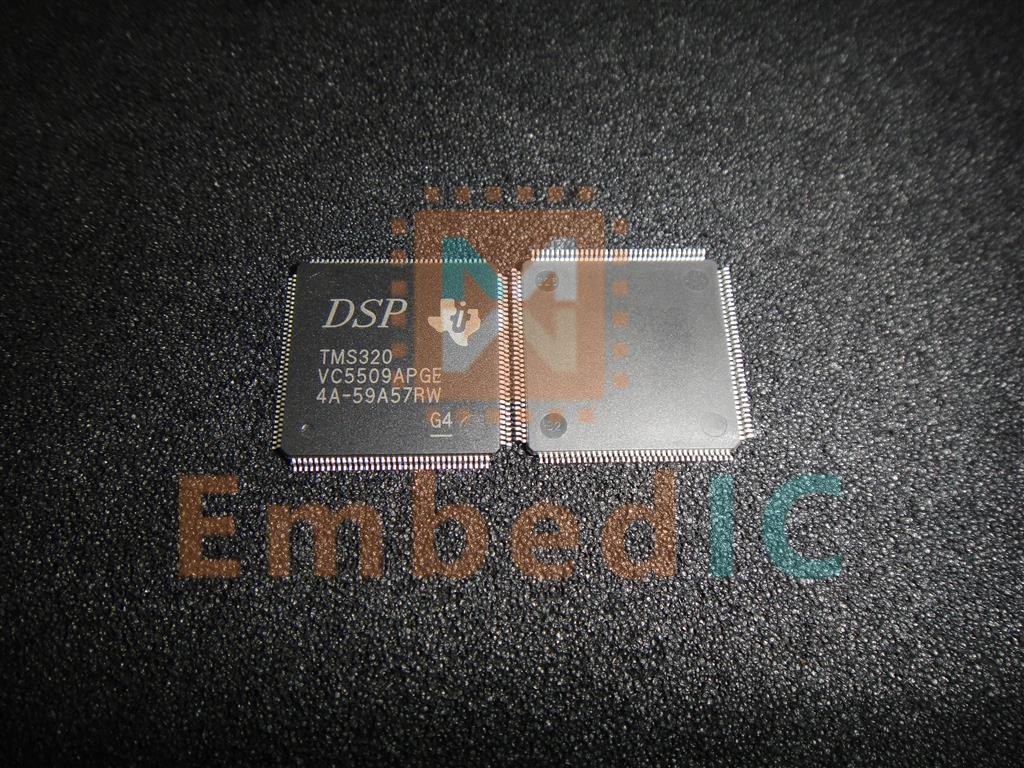
IC DSP FIX PT 16-BIT 144-LQFP
 PCB Symbol, Footprint
 Send Inquiry
 Download Datasheet
 SUPPLIERS WHOLESALE PRICE TRENDS
Price comparison from authorized distributors
 TMS320VC5509APGE Competitive Prices
EmbedIC has the unique source of supply. We can offer TMS320VC5509APGE more competitive price for our customers. You can enjoy our best service by purchasing Texas Instruments TMS320VC5509APGE, Please feel free to contact for the best price of TMS320VC5509APGE 16bit DSP. Click To Get Quotation
The TMS320VC5509A fixed-point digital signal processor (DSP) is based on the TMS320C55x DSP generation CPU processor core. The C55x? DSP architecture achieves high performance and low power through increased parallelism and total focus on reduction in power dissipation. The CPU supports an internal bus structure that is composed of one program bus, three data read buses, two data write buses, and additional buses dedicated to peripheral and DMA activity. These buses provide the ability to perform up to three data reads and two data writes in a single cycle. In parallel, the DMA controller can perform up to two data transfers per cycle independent of the CPU activity.
The C55x CPU provides two multiply-accumulate (MAC) units, each capable of 17-bit × 17-bit multiplication in a single cycle. A central 40-bit arithmetic/logic unit (ALU) is supported by an additional 16-bit ALU. Use of the ALUs is under instruction set control, providing the ability to optimize parallel activity and power consumption. These resources are managed in the Address Unit (AU) and Data Unit (DU) of the C55x CPU.
The C55x DSP generation supports a variable byte width instruction set for improved code density. The Instruction Unit (IU) performs 32-bit program fetches from internal or external memory and queues instructions for the Program Unit (PU). The Program Unit decodes the instructions, directs tasks to AU and DU resources, and manages the fully protected pipeline. Predictive branching capability avoids pipeline flushes on execution of conditional instructions.
The general-purpose input and output functions and the 10-bit A/D provide sufficient pins for status, interrupts, and bit I/O for LCDs, keyboards, and media interfaces. The parallel interface operates in two modes, either as a slave to a microcontroller using the HPI port or as a parallel media interface using the asynchronous EMIF. Serial media is supported through two MultiMedia Card/Secure Digital (MMC/SD) peripherals and three McBSPs.
The 5509A peripheral set includes an external memory interface (EMIF) that provides glueless access to asynchronous memories like EPROM and SRAM, as well as to high-speed, high-density memories such as synchronous DRAM. Additional peripherals include Universal Serial Bus (USB), real-time clock, watchdog timer, and I2C multi-master and slave interface. Three full-duplex multichannel buffered serial ports (McBSPs) provide glueless interface to a variety of industry-standard serial devices, and multichannel communication with up to 128 separately enabled channels. The enhanced host-port interface (HPI) is a 16-bit parallel interface used to provide host processor access to 32K bytes of internal memory on the 5509A. The HPI can be configured in either multiplexed or non-multiplexed mode to provide glueless interface to a wide variety of host processors. The DMA controller provides data movement for six independent channel contexts without CPU intervention, providing DMA throughput of up to two 16-bit words per cycle. Two general-purpose timers, up to eight dedicated general-purpose I/O (GPIO) pins, and digital phase-locked loop (DPLL) clock generation are also included.
The 5509A is supported by the industry‘s award-winning eXpressDSP?, Code Composer Studio? Integrated Development Environment (IDE), DSP/BIOS?, Texas Instruments’ algorithm standard, and the industry‘s largest third-party network. The Code Composer Studio IDE features code generation tools including a C Compiler and Visual Linker, simulator, RTDX?, XDS510? emulation device drivers, and evaluation modules. The 5509A is also supported by the C55x DSP Library which features more than 50 foundational software kernels (FIR filters, IIR filters, FFTs, and various math functions) as well as chip and board support libraries.
The TMS320C55x DSP core was created with an open architecture that allows the addition of application-specific hardware to boost performance on specific algorithms. The hardware extensions on the 5509A strike the perfect balance of fixed function performance with programmable flexibility, while achieving low-power consumption, and cost that traditionally has been difficult to find in the video-processor market. The extensions allow the 5509A to deliver exceptional video codec performance with more than half its bandwidth available for performing additional functions such as color space conversion, user-interface operations, security, TCP/IP, voice recognition, and text-to-speech conversion. As a result, a single 5509A DSP can power most portable digital video applications with processing headroom to spare. For more information, see the TMS320C55x Hardware Extensions for Image/Video Applications Programmer‘s Reference (literature number SPRU098). For more information on using the the DSP Image Processing Library, see the TMS320C55x Image/Video Processing Library Programmer‘s Reference (literature number SPRU037).
Symbol
Footprint
Clock Rate 200MHz
Operating Temperature -40℃ ~ 85℃ (TC)
Type Fixed Point
Non-Volatile Memory ROM (64 kB)
Package / Case 144-LQFP
Voltage - Core 1.60V
Voltage - I/O 3.00V, 3.30V
Mounting Type Surface Mount
Interface Host Interface, I2C, McBSP
Supplier Device Package 144-LQFP (20x20)
On-Chip RAM 256kB
Manufacturer: Renesas
IC MCU 32BIT 512KB FLASH 100LGA
Product Categories: 32bit MCU
Lifecycle:
RoHS:
Manufacturer: NXP
IC MCU 32BIT ROMLESS 180TFBGA
Product Categories: 32bit MCU
Lifecycle:
RoHS:
Manufacturer: Microchip
IC MCU 32BIT 512KB FLASH 100BGA
Product Categories: 32bit MCU
Lifecycle:
RoHS:
Manufacturer: Xilinx Inc.
IC SOC CORTEX-A53 1156FCBGA
Product Categories: SOC
Lifecycle:
RoHS:
Manufacturer: Cypress
IC MCU 8K LS USB/PS-2 24-DIP
Product Categories: General MCU
Lifecycle:
RoHS:
Manufacturer: Cypress
IC MCU 8K FULL SPEED USB 28SOIC
Product Categories: General MCU
Lifecycle:
RoHS:
Manufacturer: Maxim
IC MCU 16BIT 64KB FLASH 40TQFN
Product Categories: 16bit MCU
Lifecycle:
RoHS:
Manufacturer: Microchip
IC MCU 16BIT 512KB FLASH 100TQFP
Product Categories: 16bit MCU
Lifecycle:
RoHS:
Manufacturer: Silicon Labs
IC MCU 8BIT 32KB FLASH 48TQFP
Product Categories: 8bit MCU
Lifecycle:
RoHS:
Looking forward to your comment
Comment
 Popular Searches
8 Bit MCU, Flash, PIC16 Family PIC16F7XX Series Microcontrollers, 20 MHz, 7 KB, ...
EEPROM 2K 256 X 8 2.5V SERIAL EE IND
System-On-Modules - SOM RCM2200
32-bit Arm Cortex-A53 vision processor with ISP, powerful 3D GPU, dual APEX-2 v...
IC MCU 8BIT 60KB FLASH 44QFP
DSP 20MHZ 44QFP
1
2
3
4
5
6
Product updates, events, and resources in your inbox


Smart System

Traffic Management

Security

Consumer Electronics

Wireless Technology

Robot

Internet of Things

Industrial Control