Hello! Welcome to Embedic!
This website uses cookies. By using this site, you consent to the use of cookies. For more information, please take a look at our Privacy Policy.
Home > Embedded ICs > Embedded - Digital Signal Processors & Controllers (DSP, DSC) > TMS320DM8147BCYE1
Texas Instruments

TMS320DM8147BCYE1

Pictures are for reference only Please prevail in kind
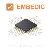
  • Quantity : *

  • Contact Name : *

  • Email : *

price SUPPLIERS WHOLESALE PRICE TRENDS

Price comparison from authorized distributors

price info TMS320DM8147BCYE1 Competitive Prices

EmbedIC has the unique source of supply. We can offer TMS320DM8147BCYE1 more competitive price for our customers. You can enjoy our best service by purchasing Texas Instruments TMS320DM8147BCYE1, Please feel free to contact for the best price of TMS320DM8147BCYE1 DSP. Click To Get Quotation

TMS320DM8147BCYE1 Overview

TMS320DM814xDaVinci video processors are highly integrated, programmable platforms that leverage the DaVinci processor technology to meet the processing needs of the following applications to name a few: HD Video Conferencing - Skype endpoints Video Surveillance DVRs IP Netcam Digital Signage Media Players and Adapters Mobile Medical Imaging Network Projectors Home Audio and Video Equipment

The device enables Original-Equipment Manufacturers (OEMs) and Original-Design Manufacturers (ODMs) to quickly bring to market devices featuring robust operating systems support, rich user interfaces, and high processing performance through the maximum flexibility of a fully integrated mixed processor solution. The device also combines programmable video and audio processing with a highly integrated peripheral set.

The TMS320DM814x DaVinci video processors also present OEMs and ODMs with new levels of processor scalability and software reuse. An OEM or ODM that used the AM387x processors in a design and can make a similar product with added features could scale up to the pin-compatible and software-compatible TMS320DM814x processors from TI. The TMS320DM814x DaVinci video processors add a powerful C674x DSP core along with a video encoder and decoder to the hardware on the AM38x. Additionally, OEMs or ODMs that have used the AM387x or DM814x processors and find a need for a faster ARM and DSP core performance could scale up to the software-compatible AM389x or TMS320DM816x devices with higher core speeds.

Programmability is provided by an ARM Cortex-A8 RISC CPU with Neon extension, TI C674x VLIW floating-point DSP core, and high-definition video and imaging coprocessors. The ARM lets developers keep control functions separate from A/V algorithms programmed on the DSP and coprocessors, thus reducing the complexity of the system software. The ARM Cortex-A8 32-Bit RISC Core with Neon floating-point extension includes: 32KB of Instruction cache; 32KB of Data cache; 512KB of L2 Cache; 48KB of Boot ROM; and 64KB of RAM.

The rich peripheral set provides the ability to control external peripheral devices and communicate with external processors. For details on each of the peripherals, see the related sections in this document and the associated peripheral reference guides. The peripheral set includes:HD Video Processing Subsystem Dual Port Gigabit Ethernet MACs (10/100/1000 Mbps) [Ethernet Switch] with MII/RMII/GMII/RGMII and MDIO interface supporting IEEE 1588 Time-Stamping and Industrial Ethernet ProtocolsTwo USB ports with integrated 2.0 PHY PCIe x1 GEN2 Compliant interfaceTwo 10-serializer McASP audio serial ports (with DIT mode)Four quad-serilaizer McASP audio serial ports (with DIT mode)One McBSP multichannel buffered serial portSix UARTs with IrDA and CIR supportFour SPI serial interfacesThree MMC/SD/SDIO serial interfacesFour I2C master and slave interfaces Parallel Camera Interface (CAM)Up to 128 General-Purpose I/Os (GPIOs)Eight 32-bit general-purpose timers System watchdog timer Dual DDR2, and DDR3 SDRAM interfacesFlexible 8- or 16-bit asynchronous memory interfaceTwo Controller Area Network (DCAN) modulesSpin LockMailboxSerial Hard Disk Drive Interface (SATA 300)

The TMS320DM814x DaVinci video processorsalso include a high-definition video and imaging coprocessor 2 (HDVICP2), and an SGX530 3D graphics engine to off-load many video and imaging processing tasks from the DSP core, making more DSP MIPS available for common video and imaging algorithms. Additionally, it has a complete set of development tools for both the ARM and DSP, which include C compilers, a DSP assembly optimizer to simplify programming and scheduling, and a Microsoft? Windows? debugger interface for visibility into source code execution.

The C674x DSP core is the high-performance floating-point DSP generation in the TMS320C6000 DSP platform and is code-compatible with previous generation C64x Fixed-Point and C67x Floating-Point DSP generation. The C674x Floating-Point DSP processor uses 32KB of L1 program memory with EDC and 32KB of L1 data memory. Up to 32KB of L1P can be configured as program cache. The remaining memory is noncacheable no-wait-state program memory. Up to 32KB of L1D can be configured as data cache. The remaining memory is noncacheable no-wait-state data memory. The DSP has 256KB of L2 RAM with ECC, which can be defined as SRAM, L2 cache, or a combination of both. All C674x L3 and off-chip memory accesses are routed through an MMU.

Features

  • High-Performance DaVinci Video Processors
    • Up to 1-GHz ARM Cortex-A8 RISC Core
    • Up to 750-MHz C674x VLIW DSP
    • Up to 6000 MIPS and 4500 MFLOPS
    • Fully Software-Compatible with C67x+, C64x+
  • ARM Cortex-A8 Core
    • ARMv7 Architecture
      • In-Order, Dual-Issue, Superscalar Processor Core
      • Neon Multimedia Architecture
      • Supports Integer and Floating Point
      • Jazelle RCT Execution Environment
  • ARM Cortex-A8 Memory Architecture
    • 32KB of Instruction and Data Caches
    • 512KB of L2 Cache
    • 64KB of RAM, 48KB of Boot ROM
  • TMS320C674x Floating-Point VLIW DSP
    • 64 General-Purpose Registers (32-Bit)
    • Six ALU (32-/40-Bit) Functional Units
      • Supports 32-Bit Integer, SP (IEEE Single Precision/32-Bit) and DP (IEEE Double Precision/64-Bit) Floating Point
      • Supports up to Four SP Adds Per Clock and Four DP Adds Every Two Clocks
      • Supports up to Two Floating-Point (SP or DP) Approximate Reciprocal or Square Root Operations Per Cycle
    • Two Multiply Functional Units
      • Mixed-Precision IEEE Floating-Point Multiply Supported up to:
        • 2 SP x SP → SP Per Clock
        • 2 SP x SP → DP Every Two Clocks
        • 2 SP x DP → DP Every Three Clocks
        • 2 DP x DP → DP Every Four Clocks
      • Fixed-Point Multiply Supports Two 32 x 32 Multiplies, Four 16 x 16-Bit Multiplies Including Complex Multiplies, or Eight 8 x 8-Bit Multiplies per Clock Cycle
  • C674x Two-Level Memory Architecture
    • 32KB of L1P RAM/Cache With EDC
    • 32KB of L1D RAM/Cache
    • 256KB of L2 Unified Mapped RAM/Caches With ECC
  • System Memory Management Unit (MMU)
    • Maps C674x DSP and EDMA TC Memory Accesses to System Addresses
  • 128KBof On-Chip Memory Controller (OCMC) RAM
  • Imaging Subsystem (ISS)
    • Camera Sensor Connection
      • Parallel Connection for Raw (up to 16-Bit) and BT.656 or BT.1120 (8- and 16-Bit)
    • Image Sensor Interface (ISIF) for Handling Image and Video Data From the Camera Sensor
    • Resizer
      • Resizing Image and Video From 1/16x to 8x
      • Generating Two Different Resizing Outputs Concurrently
  • Programmable High-Definition Video Image Coprocessing (HDVICP v2) Engine
    • Encode, Decode, Transcode Operations
    • H.264, MPEG-2, VC-1, MPEG-4, SP/ASP, JPEG/MJPEG
  • Media Controller
    • Controls the HDVPSS, HDVICP2, and ISS
  • SGX530 3D Graphics Engine
    • Delivers up to 25 MPoly/sec
    • Universal Scalable Shader Engine
    • Direct3D Mobile, OpenGLES 1.1 and 2.0, OpenVG 1.0, OpenMax API Support
    • Advanced Geometry DMA Driven Operation
    • Programmable HQ Image Anti-Aliasing
  • Endianness
    • ARM and DSP Instructions/Data – Little Endian
  • HD Video Processing Subsystem (HDVPSS)
    • Two 165-MHz, 2-channel HD Video Capture Modules
      • One 16-/24-Bit Input or Dual 8-Bit SD Input Channels
      • One 8-/16-/24-Bit Input and One 8-Bit Only Input Channels
    • Two 165-MHz HD Video Display Outputs
      • One 16-, 24-, or 30-Bit Output and One 16- or 24-Bit Output
    • Composite or S-Video Analog Output
    • Macrovision Support Available
    • Digital HDMI 1.3 Transmitter With Integrated PHY
    • Advanced Video Processing Features Such as Scan, Format, Rate Conversion
    • Three Graphics Layers and Compositors
  • Dual 32-Bit DDR2/DDR3 SDRAM Interfaces
    • Supports up to DDR2-800 and DDR3-1066
    • Up to Eight x 8 Devices Total 2GB of Total Address Space
    • Dynamic Memory Manager (DMM)
      • Programmable Multi-Zone Memory Mapping and Interleaving
      • Enables Efficient 2D Block Accesses
      • Supports Tiled Objects in 0°, 90°, 180°, or 270° Orientation and Mirroring
      • Optimizes Interlaced Accesses
  • General-Purpose Memory Controller (GPMC)
    • 8- or 16-Bit Multiplexed Address and Data Bus
    • 512MB of Address Space Divided Among up to 8 Chip Selects
    • Glueless Interface to NOR Flash, NAND Flash (BCH/Hamming Error Code Detection), SRAM and Pseudo-SRAM
    • Error Locator Module (ELM) Outside of GPMC to Provide Up to 16-Bit or 512-Byte Hardware ECC for NAND
    • Flexible Asynchronous Protocol Control for Interface to FPGA, CPLD, ASICs, and so Forth
  • Enhanced Direct Memory Access (EDMA) Controller
    • Four Transfer Controllers
    • 64 Independent DMA Channels and 8 Independent QDMA Channels
  • Dual Port Ethernet (10/100/1000 Mbps) With Optional Switch
    • IEEE 802.3 Compliant (3.3-V I/O Only)
    • MII/RMII/GMII/RGMII Media Independent Interfaces
    • Management Data I/O (MDIO) Module
    • Reset Isolation
    • IEEE 1588 Time-Stamping and Industrial Ethernet Protocols
  • Dual USB 2.0 Ports With Integrated PHYs
    • USB2.0 High- and Full-Speed Clients
    • USB2.0 High-, Full-, and Low-Speed Hosts, or OTG
    • Supports End Points 0–15
  • One PCI Express 2.0 Port With Integrated PHY
    • Single Port With One Lane at 5.0 GT/s
    • Configurable as Root Complex or Endpoint
  • Eight 32-Bit General-Purpose Timers (Timer1–8)
  • One System Watchdog Timer (WDT0)
  • Six Configurable UART/IrDA/CIR Modules
    • UART0 With Modem Control Signals
    • Supports up to 3.6864 Mbps UART0/1/2
    • Supports up to 12 Mbps UART3/4/5
    • SIR, MIR, FIR (4.0 MBAUD), and CIR
  • Four Serial Peripheral Interfaces (SPIs) (up to
    48 MHz)
    • Each With Four Chip Selects
  • Three MMC/SD/SDIO Serial Interfaces (up to
    48 MHz)
    • Three Supporting up to 1-, 4-, or 8-Bit Modes
  • Dual Controller Area Network (DCAN) Modules
    • CAN Version 2 Part A, B
  • Four Inter-Integrated Circuit (I2C Bus) Ports
  • Six Multichannel Audio Serial Ports (McASPs)
    • Dual Ten Serializer Transmit and Receive Ports
    • Quad Four Serializer Transmit and Receive Ports
    • DIT-Capable For S/PDIF (All Ports)
  • Multichannel Buffered Serial Port (McBSP)
    • Transmit and Receive Clocks up to 48 MHz
    • Two Clock Zones and Two Serial Data Pins
    • Supports TDM, I2S, and Similar Formats
  • Serial ATA (SATA) 3.0 Gbps Controller With Integrated PHY
    • Direct Interface to One Hard Disk Drive
    • Hardware-Assisted Native Command Queuing (NCQ) from up to 32 Entries
    • Supports Port Multiplier and Command-Based Switching
  • Real-Time Clock (RTC)
    • One-Time or Periodic Interrupt Generation
  • Up to 128 General-Purpose I/O (GPIO) Pins
  • One Spin Lock Module with up to 128 Hardware Semaphores
  • One Mailbox Module with 12 Mailboxes
  • On-Chip ARM ROM Bootloader (RBL)
  • Power, Reset, and Clock Management
    • Multiple Independent Core Power Domains
    • Multiple Independent Core Voltage Domains
    • Support for Three Operating Points (OPP100, OPP120, OPP166) per Voltage Domain
    • Clock Enable and Disable Control for Subsystems and Peripherals
  • 32KB of Embedded Trace Buffer (ETB) and
    5-Pin Trace Interface for Debug
  • IEEE 1149.1 (JTAG) Compatible
  • 684-Pin Pb-Free BGA Package (CYE Suffix), 0.8-mm Ball Pitch With Via Channel Technology to Reduce PCB Cost
  • 45-nm CMOS Technology
  • 1.8- and 3.3-V Dual Voltage Buffers for General I/O

Applications

DM81x Video SOC, DaVinci?

Specifications

  • Clock Rate 700MHz DSP, 1GHz ARM

  • Operating Temperature 0℃ ~ 90℃ (TJ)

  • Type Digital Media System-on-Chip (DMSoC)

  • Non-Volatile Memory ROM (48 kB)

  • Package / Case 684-BFBGA, FCBGA

  • Voltage - Core 1.1V, 1.2V, 1.35V

  • Voltage - I/O 1.5V, 1.8V, 3.3V

  • Mounting Type Surface Mount

  • Interface CAN, Ethernet, I2C, McASP, McBSP, MMC/SD/SDIO, SATA, SPI, UART, USB

  • Supplier Device Package 684-FCBGA (23x23)

  • On-Chip RAM 1.08MB

Popular Products

  • PIC18LF2682T-I/SO

    Manufacturer: Microchip

    IC MCU 8BIT 80KB FLASH 28SOIC

    Product Categories: 8bit MCU

    Lifecycle:

    RoHS:

  • M2S050T-1FGG896

    Manufacturer: Microsemi Corporation

    IC SOC CORTEX-M3 166MHZ 896FBGA

    Product Categories: SOC

    Lifecycle:

    RoHS:

  • M2S060TS-1VFG400I

    Manufacturer: Microsemi Corporation

    IC SOC CORTEX-M3 166MHZ 400VFBGA

    Product Categories: SOC

    Lifecycle:

    RoHS:

  • CY8C20075-24LKXI

    Manufacturer: Cypress

    IC CAPSENSE 8K FLASH 16 QFN

    Product Categories: 8bit MCU

    Lifecycle:

    RoHS:

  • PIC32MX320F032HT-40V/MR

    Manufacturer: Microchip

    IC MCU 32BIT 32KB FLASH 64QFN

    Product Categories: 32bit MCU

    Lifecycle:

    RoHS:

  • M2S060TS-FGG676I

    Manufacturer: Microsemi Corporation

    IC SOC CORTEX-M3 166MHZ 676FBGA

    Product Categories: SOC

    Lifecycle:

    RoHS:

  • PIC16LC73A-04I/SO

    Manufacturer: Microchip

    IC MCU 8BIT 7KB OTP 28SOIC

    Product Categories: 8bit MCU

    Lifecycle:

    RoHS:

  • M2S060TS-1FGG676I

    Manufacturer: Microsemi Corporation

    IC SOC CORTEX-M3 166MHZ 676FBGA

    Product Categories: SOC

    Lifecycle:

    RoHS:

  • DSPIC33EP64GS502T-E/MM

    Manufacturer: Microchip

    IC MCU 16BIT 64KB FLASH 28QFN

    Product Categories: 16bit MCU

    Lifecycle:

    RoHS:

Product evaluation

  • Looking forward to your comment

  • Comment

    Verification Code * 

Compare products

Compare Empty