Hello! Welcome to Embedic!


Pictures are for reference only Please prevail in kind
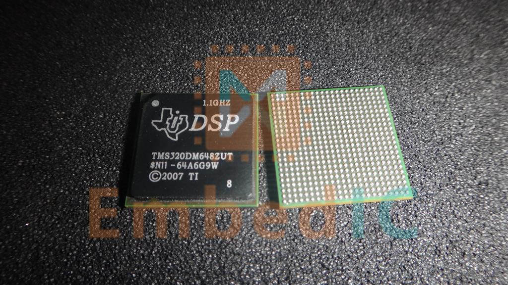
IC DGTL MEDIA PROC 529FCBGA
 PCB Symbol, Footprint
 Send Inquiry
 Download Datasheet
 SUPPLIERS WHOLESALE PRICE TRENDS
Price comparison from authorized distributors
 TMS320DM648ZUT1 Competitive Prices
EmbedIC has the unique source of supply. We can offer TMS320DM648ZUT1 more competitive price for our customers. You can enjoy our best service by purchasing Texas Instruments TMS320DM648ZUT1, Please feel free to contact for the best price of TMS320DM648ZUT1 DSP. Click To Get Quotation
The TMS320C64x+? DSPs (including the TMS320DM647/TMS320DM648 devices) are the highest-performance fixed-point DSP generation in the TMS320C6000? DSP platform. The DM647, DM648 devices are based on the third-generation high-performance, advanced VelociTI? very-long-instruction-word (VLIW) architecture developed by Texas Instruments (TI), making these DSPs an excellent choice for digital media applications. The C64x+? devices are upward code-compatible from previous devices that are part of the C6000? DSP platform. The C64x? DSPs support added functionality and have an expanded instruction set from previous devices.
Any reference to the C64x DSP or C64x CPU also applies, unless otherwise noted, to the C64x+ DSP and C64x+ CPU, respectively.
With performance of up to 8800 million instructions per second (MIPS) at a clock rate of 1.1 GHz, the C64x+ core offers solutions to high-performance DSP programming challenges. The DSP core possesses the operational flexibility of high-speed controllers and the numerical capability of array processors. The C64x+ DSP core processor has 64 general-purpose registers of 32-bit word length and eight highly independent functional units—two multipliers for a 32-bit result and six arithmetic logic units (ALUs). The eight functional units include instructions to accelerate the performance in video and imaging applications. The DSP core can produce four 16-bit multiply-accumulates (MACs) per cycle for up to 4400 million MACs per second (MMACS), or eight 8-bit MACs per cycle for up tp 8800 MMACS. For more details on the C64x+ DSP, see the (literature number SPRU732).
The devices also have application-specific hardware logic, on-chip memory, and additional on-chip peripherals similar to the other C6000 DSP platform devices. The core uses a two-level cache-based architecture. The Level 1 program cache (L1P) is a 256K-bit direct mapped cache and the Level 1 data cache (L1D) is a 256K-bit 2-way set-associative cache. The Level 2 memory/cache (L2) consists of a 4M-bit (DM648) or 2M-bit (DM647)memory space that is shared between program and data space. L2 memory can be configured as mapped memory, cache, or combinations of the two.
The peripheral set includes five configurable 16-bit video port peripherals (VP0, VP1, VP2, VP3, and VP4). These video port peripherals provide a glueless interface to common video decoder and encoder devices. The video port peripherals support multiple resolutions and video standards (e.g., CCIR601, ITU-BT.656, BT.1120, SMPTE 125M, 260M, 274M, and 296M), a VCXO interpolated control port (VIC); a 1000 Mbps Ethernet Switch Subsystem with a management data input/output (MDIO) module and two SGMII ports (DM648) or one SGMII port (only DM647); a 4-bit transmit, 4-bit receive VLYNQ interface; an inter-integrated circuit (I2C) bus interface; a multichannel audio serial port (McASP) with ten serializers; four 64-bit general-purpose timers each configurable as two independent 32-bit timers; a user-configurable 16-bit or 32-bit host-port interface (HPI); 32 pins for general-purpose input/output (GPIO) with programmable interrupt/event generation modes, multiplexed with other peripherals; one UART; and two glueless external memory interfaces: a synchronous and asynchronous external memory interface (EMIFA) for slower memories/peripherals, and a higher DDR2 SDRAM interface.
The video port peripherals provide a glueless interface to common video decoder and encoder devices. The video port peripherals support multiple resolutions and video standards (e.g., CCIR601, ITU-BT.656, BT.1120, SMPTE 125M, 260M, 274M, and 296M).
The video port peripherals are configurable and can support either video capture and/or video display modes. Each video port consists of two channels (A and B) with a 5120-byte capture/display buffer that is splittable between the two channels.
For more details on the video port peripherals, see the(literature number SPRUEM1).
The management data input/output (MDIO) module continuously polls all 32 MDIO addresses to enumerate all PHY devices in the system.
The I2C and VLYNQ ports allow the device to easily control peripheral modules and/or communicate with host processors.
The rich peripheral set provides the ability to control external peripheral devices and communicate with external processors. For details on each of the peripherals, see the related sections later in this document and the associated peripheral reference guides.
The devices have a complete set of development tools. These include C compilers, a DSP assembly optimizer to simplify programming and scheduling, and a Windows? debugger interface for visibility into source code execution.
Clock Rate 1.1GHz
Operating Temperature 0℃ ~ 90℃ (TC)
Type Fixed Point
Non-Volatile Memory ROM (64 kB)
Package / Case 529-BFBGA, FCBGA
Voltage - Core 1.20V
Voltage - I/O 1.8V, 3.3V
Mounting Type Surface Mount
Interface Host Interface, I2C, McASP, PCI, SPI, UART
Supplier Device Package 529-FCBGA (19x19)
On-Chip RAM 576kB
Manufacturer: Texas Instruments
IC MCU 16BIT 64KB FRAM 64VQFN
Product Categories: 16bit MCU
Lifecycle:
RoHS:
Manufacturer: ROHM
IC MCU 8BIT 16KB FLASH 100TQFP
Product Categories: 8bit MCU
Lifecycle:
RoHS:
Manufacturer: Renesas
IC MCU 16BIT 16KB FLASH 32LQFP
Product Categories: 16bit MCU
Lifecycle:
RoHS:
Manufacturer: Microsemi Corporation
IC SOC CORTEX-M3 166MHZ 400VFBGA
Product Categories: SOC
Lifecycle:
RoHS:
Manufacturer: Microchip
IC MCU 8BIT 1.5KB OTP 18SOIC
Product Categories: 8bit MCU
Lifecycle:
RoHS:
Manufacturer: Microsemi Corporation
IC SOC CORTEX-M3 166MHZ 676FBGA
Product Categories: SOC
Lifecycle:
RoHS:
Manufacturer: Microsemi Corporation
IC SOC CORTEX-M3 166MHZ 325BGA
Product Categories: SOC
Lifecycle:
RoHS:
Manufacturer: Microchip
IC MCU 8BIT 3.5KB OTP 18SOIC
Product Categories: 8bit MCU
Lifecycle:
RoHS:
Looking forward to your comment
Comment
 Popular Searches
8 Bit MCU, Flash, PIC16 Family PIC16F7XX Series Microcontrollers, 20 MHz, 7 KB, ...
EEPROM 2K 256 X 8 2.5V SERIAL EE IND
System-On-Modules - SOM RCM2200
32-bit Arm Cortex-A53 vision processor with ISP, powerful 3D GPU, dual APEX-2 v...
IC MCU 8BIT 60KB FLASH 44QFP
DSP 20MHZ 44QFP
1
2
3
4
5
6
Product updates, events, and resources in your inbox


Smart System

Traffic Management

Security

Consumer Electronics

Wireless Technology

Robot

Internet of Things

Industrial Control