Hello! Welcome to Embedic!

Pictures are for reference only Please prevail in kind
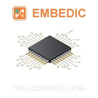
IC DGTL MEDIA SOC 529FCBGA
 PCB Symbol, Footprint
 Send Inquiry
 Download Datasheet
 SUPPLIERS WHOLESALE PRICE TRENDS
Price comparison from authorized distributors
 TMS320DM6467CCUTA6 Competitive Prices
EmbedIC has the unique source of supply. We can offer TMS320DM6467CCUTA6 more competitive price for our customers. You can enjoy our best service by purchasing Texas Instruments TMS320DM6467CCUTA6, Please feel free to contact for the best price of TMS320DM6467CCUTA6 SOC. Click To Get Quotation
The TMS320DM6467 (also referenced as DM6467) leverages TI's DaVinci?technology to meet the networked media encode and decode digital media processingneeds of next-generation embedded devices.
The DM6467 enables OEMs and ODMs to quickly bring to market devices featuringrobust operating systems support, rich user interfaces, high processingperformance, and long battery life through the maximum flexibility of a fullyintegrated mixed processor solution.
The dual-core architecture of the DM6467 provides benefits of both DSP andReduced Instruction Set Computer (RISC) technologies, incorporating ahigh-performance TMS320C64x+ DSP core and an ARM926EJ-S core.
The ARM926EJ-S is a 32-bit RISC processor core that performs 32-bit or 16-bitinstructions and processes 32-bit, 16-bit, or 8-bit data. The core usespipelining so that all parts of the processor and memory system can operatecontinuously.
The ARM core incorporates:
The TMS320C64x+? DSPs are the highest-performance fixed-point DSP generationin the TMS320C6000? DSP platform. It is based on an enhanced version of thesecond-generation high-performance, advanced very-long-instruction-word (VLIW)architecture developed by Texas Instruments (TI), making these DSP cores anexcellent choice for digital media applications. The C64x is a code-compatiblemember of the C6000? DSP platform. The TMS320C64x+ DSP is an enhancement of theC64x+ DSP with added functionality and an expanded instruction set.
Any reference to the C64x DSP or C64x CPU also applies, unless otherwisenoted, to the C64x+ DSP and C64x+ CPU, respectively.
With performance of up to 5832 million instructions per second (MIPS) at aclock rate of 729 MHz, the C64x+ core offers solutions to high-performance DSPprogramming challenges. The DSP core possesses the operational flexibility ofhigh-speed controllers and the numerical capability of array processors. TheC64x+ DSP core processor has 64 general-purpose registers of 32-bit word lengthand eight highly independent functional units-two multipliers for a 32-bitresult and six arithmetic logic units (ALUs). The eight functional units includeinstructions to accelerate the performance in video and imaging applications.The DSP core can produce four 16-bit multiply-accumulates (MACs) per cycle for atotal of 2376 million MACs per second (MMACS), or eight 8-bit MACs per cycle fora total of 4752 MMACS. For more details on the C64x+ DSP, see theTMS320C64x/C64x+ DSP CPU and Instruction Set Reference Guide(literaturenumber SPRU732).
The DM6467 also has application-specific hardware logic, on-chip memory, andadditional on-chip peripherals similar to the other C6000 DSP platform devices.The DM6467 core uses a two-level cache-based architecture. The Level 1 programcache (L1P) is a 256K-bit direct mapped cache and the Level 1 data cache (L1D)is a 640K-bit 2-way set-associative cache. The Level 2 memory/cache (L2)consists of an 512K-bit memory space that is shared between program and dataspace. L2 memory can be configured as mapped memory, cache, or combinations ofthe two.
The peripheral set includes: a configurable video port; a 10/100/1000 Mb/sEthernet MAC (EMAC) with a Management Data Input/Output (MDIO) module; a 4-bittransfer/4-bit receive VLYNQ interface; an inter-integrated circuit (I2C) Businterface; a multichannel audio serial port (McASP0) with 4 serializers; asecondary multichannel audio serial port (McASP1) with a single transmitserializer; 2 64-bit general-purpose timers each configurable as 2 independent32-bit timers; 1 64-bit watchdog timer; a configurable 32-bit host portinterface (HPI); up to 33-pins of general-purpose input/output (GPIO) withprogrammable interrupt/event generation modes, multiplexed with otherperipherals; 3 UART/IrDA/CIR interfaces with modem interface signals on UART0; 2pulse width modulator (PWM) peripherals; an ATA/ATAPI-6 interface; a 33-MHzperipheral component interface (PCI); and 2 external memory interfaces: anasynchronous external memory interface (EMIFA) for slower memories/peripherals,and a higher speed synchronous memory interface for DDR2.
The Ethernet Media Access Controller (EMAC) provides an efficient interfacebetween the DM6467 and the network. The DM6467 EMAC support both 10Base-T and100Base-TX, or 10 Mbits/second (Mbps) and 100 Mbps in either half- orfull-duplex mode; and 1000Base-TX (1 Gbps) in full-duplex mode with hardwareflow control and quality of service (QOS) support.
The Management Data Input/Output (MDIO) module continuously polls all 32 MDIOaddresses in order to enumerate all PHY devices in the system. Once a PHYcandidate has been selected by the ARM, the MDIO module transparently monitorsits link state by reading the PHY status register. Link change events are storedin the MDIO module and can optionally interrupt the ARM, allowing the ARM topoll the link status of the device without continuously performing costly MDIOaccesses.
The PCI, HPI, I2C, SPI, USB2.0, and VLYNQ ports allow the DM6467 to easilycontrol peripheral devices and/or communicate with host processors.
The DM6467 also includes a High-Definition Video/Imaging Co-processor(HDVICP) and Video Data Conversion Engine (VDCE) to offload many video andimaging processing tasks from the DSP core, making more DSP MIPS available forcommon video and imaging algorithms. For more information on the HDVICP enhancedcodecs, such as H.264 and MPEG4, please contact your nearest TI salesrepresentative.
The rich peripheral set provides the ability to control external peripheraldevices and communicate with external processors. For details on each of theperipherals, see the related sections later in this document and the associatedperipheral reference guides.
The DM6467 has a complete set of development tools for both the ARM and DSP.These include C compilers, a DSP assembly optimizer to simplify programming andscheduling, and a Windows? debugger interface for visibility into source code
Operating Temperature -40℃ ~ 105℃ (TC)
Type Digital Media System-on-Chip (DMSoC)
Non-Volatile Memory ROM (8 kB)
Package / Case 529-BFBGA, FCBGA
Voltage - Core 1.20V
Voltage - I/O 1.8V, 3.3V
Mounting Type Surface Mount
Interface EBI/EMI, Ethernet, HPI, I2C, McASP, PCI, SPI, UART, USB
Supplier Device Package 529-FCBGA (19x19)
On-Chip RAM 248kB
Manufacturer: Intel
IC SOC CORTEX-A9 800MHZ 1152FBGA
Product Categories: SOC
Lifecycle:
RoHS:
Manufacturer: STMicroelectronics
IC MCU 32BIT 1MB FLASH 144LQFP
Product Categories: 32bit MCU
Lifecycle:
RoHS:
Manufacturer: Intel
IC SOC CORTEX-A9 1.5GHZ 1152FBGA
Product Categories: SOC
Lifecycle:
RoHS:
Manufacturer: Intel
IC SOC CORTEX-A9 800MHZ 1517FBGA
Product Categories: SOC
Lifecycle:
RoHS:
Manufacturer: Intel
IC SOC CORTEX-A9 1.5GHZ 1152FBGA
Product Categories: SOC
Lifecycle:
RoHS:
Manufacturer: STMicroelectronics
IC MCU 32BIT 1MB FLASH 216TFBGA
Product Categories: 32bit MCU
Lifecycle:
RoHS:
Manufacturer: Microchip
IC MCU 32BIT 2MB FLASH 144TFBGA
Product Categories: 32bit MCU
Lifecycle:
RoHS:
Manufacturer: Intel
IC SOC CORTEX-A9 800MHZ 1517FBGA
Product Categories: SOC
Lifecycle:
RoHS:
Looking forward to your comment
Comment
 Popular Searches
8 Bit MCU, Flash, PIC16 Family PIC16F7XX Series Microcontrollers, 20 MHz, 7 KB, ...
EEPROM 2K 256 X 8 2.5V SERIAL EE IND
System-On-Modules - SOM RCM2200
32-bit Arm Cortex-A53 vision processor with ISP, powerful 3D GPU, dual APEX-2 v...
IC MCU 8BIT 60KB FLASH 44QFP
DSP 20MHZ 44QFP
1
2
3
4
5
6
Product updates, events, and resources in your inbox


Smart System

Traffic Management

Security

Consumer Electronics

Wireless Technology

Robot

Internet of Things

Industrial Control