Hello! Welcome to Embedic!
This website uses cookies. By using this site, you consent to the use of cookies. For more information, please take a look at our Privacy Policy.
Home > Embedded ICs > Embedded - Microprocessor Unit (MPU) > OMAP3530ECBBA
Texas Instruments

OMAP3530ECBBA

Pictures are for reference only Please prevail in kind
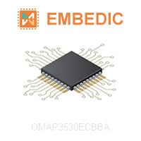
  • Quantity : *

  • Contact Name : *

  • Email : *

price SUPPLIERS WHOLESALE PRICE TRENDS

Price comparison from authorized distributors

price info OMAP3530ECBBA Competitive Prices

EmbedIC has the unique source of supply. We can offer OMAP3530ECBBA more competitive price for our customers. You can enjoy our best service by purchasing Texas Instruments OMAP3530ECBBA, Please feel free to contact for the best price of OMAP3530ECBBA MPU. Click To Get Quotation

OMAP3530ECBBA Overview

OMAP3530 and OMAP3525devices are based on the enhanced OMAP 3 architecture.

The OMAP 3 architecture is designed to provide best-in-class video, image, and graphics processing sufficient to support the following:

  • Streaming video
  • Video conferencing
  • High-resolution still image

The device supports high-level operating systems (HLOSs), such as:

  • Linux?
  • Windows? CE
  • Android?

This OMAP device includes state-of-the-art power-management techniques required for high-performance mobile products.

The following subsystems are part of the device:

  • Microprocessor unit (MPU) subsystem based on the ARM Cortex-A8 microprocessor
  • IVA2.2 subsystem with a C64x+ digital signal processor (DSP) core
  • PowerVR SGX subsystem for 3D graphics acceleration to support display (OMAP3530 device only)
  • Camera image signal processor (ISP) that supports multiple formats and interfacing options connected to a wide variety of image sensors
  • Display subsystem with a wide variety of features for multiple concurrent image manipulation, and a programmable interface supporting a wide variety of displays. The display subsystem also supports NTSC and PAL video out.
  • Level 3 (L3) and level 4 (L4) interconnects that provide high-bandwidth data transfers for multiple initiators to the internal and external memory controllers and to on-chip peripherals

The device also offers:

  • A comprehensive power- and clock-management scheme that enables high-performance, low-power operation, and ultralow-power standby features. The device also supports SmartReflex adaptative voltage control. This power-management technique for automatic control of the operating voltage of a module reduces the active power consumption.
  • Memory-stacking feature using the package-on-package (POP) implementation (CBB and CBC packages only)

OMAP3530 and OMAP3525 devices are available in a 515-pin s-PBGA package (CBB suffix), 515-pin s-PBGA package (CBC suffix), and a 423-pin s-PBGA package (CUS suffix). Some features of the CBB and CBC packages are not available in the CUS package. (See Table 1-1 for package differences).

This data manual presents the electrical and mechanical specifications for the OMAP3530 and OMAP3525 applications processors. The information in this data manual applies to both the commercial and extended temperature versions of the OMAP3530 and OMAP3525 applications processors unless otherwise indicated. This data manual consists of the following sections:

  • Section 2: Terminal Description: assignment, electrical characteristics, multiplexing, and functional description
  • Section 3: Electrical Characteristics: power domains, operating conditions, power consumption, and DC characteristics
  • Section 4: Clock Specifications input and output clocks, DPLL and DLL
  • Section 5: Video Dac Specifications
  • Section 6: Timing Requirements and Switching Characteristics
  • Section 7: Package Characteristics: thermal characteristics, device nomenclature, and mechanical data for available packaging

Features

  • OMAP3530 and OMAP3525 Devices:
    • OMAP 3 Architecture
    • MPU Subsystem
      • Up to 720-MHz ARM Cortex-A8 Core
      • NEON SIMD Coprocessor
    • High-Performance Image, Video, Audio (IVA2.2) Accelerator Subsystem
      • Up to 520-MHz TMS320C64x+ DSP Core
      • Enhanced Direct Memory Access (EDMA) Controller (128 Independent Channels)
      • Video Hardware Accelerators
    • PowerVR SGX Graphics Accelerator (OMAP3530 Device Only)
      • Tile-Based Architecture Delivering up to 10 MPoly/sec
      • Universal Scalable Shader Engine: Multi-threaded Engine Incorporating Pixel and Vertex Shader Functionality
      • Industry Standard API Support: OpenGLES 1.1 and 2.0, OpenVG1.0
      • Fine-Grained Task Switching, Load Balancing, and Power Management
      • Programmable High-Quality Image Anti-Aliasing
    • Fully Software-Compatible with C64x and ARM9
    • Commercial and Extended Temperature Grades
  • Advanced Very-Long-Instruction-Word (VLIW) TMS320C64x+ DSP Core
    • Eight Highly Independent Functional Units
      • Six ALUs (32- and 40-Bit), Each Supports Single 32-Bit, Dual 16-Bit, or Quad 8-Bit Arithmetic per Clock Cycle
      • Two Multipliers Support Four 16 x 16-Bit Multiplies (32-Bit Results) per Clock Cycle or Eight 8 x 8-Bit Multiplies (16-Bit Results) per Clock Cycle
    • Load-Store Architecture with Nonaligned Support
    • 64 32-Bit General-Purpose Registers
    • Instruction Packing Reduces Code Size
    • All Instructions Conditional
    • Additional C64x+ Enhancements
      • Protected Mode Operation
      • Exceptions Support for Error Detection and Program Redirection
      • Hardware Support for Modulo Loop Operation
  • C64x+ L1 and L2 Memory Architecture
    • 32KB of L1P Program RAM and Cache (Direct Mapped)
    • 80KB of L1D Data RAM and Cache (2-Way Set-Associative)
    • 64KB of L2 Unified Mapped RAM and Cache (4-Way Set-Associative)
    • 32KB of L2 Shared SRAM and 16KB of L2 ROM
  • C64x+ Instruction Set Features
    • Byte-Addressable (8-, 16-, 32-, and 64-Bit Data)
    • 8-Bit Overflow Protection
    • Bit Field Extract, Set, Clear
    • Normalization, Saturation, Bit-Counting
    • Compact 16-Bit Instructions
    • Additional Instructions to Support Complex Multiplies
  • ARM Cortex-A8 Core
    • ARMv7 Architecture
      • TrustZone
      • Thumb-2
      • MMU Enhancements
    • In-Order, Dual-Issue, Superscalar Microprocessor Core
    • NEON Multimedia Architecture
    • Over 2x Performance of ARMv6 SIMD
    • Supports Both Integer and Floating-Point SIMD
    • Jazelle RCT Execution Environment Architecture
    • Dynamic Branch Prediction with Branch Target Address Cache, Global History Buffer, and 8-Entry Return Stack
    • Embedded Trace Macrocell (ETM) Support for Noninvasive Debug
  • ARM Cortex-A8 Memory Architecture:
    • 16-KB Instruction Cache (4-Way Set-Associative)
    • 16-KB Data Cache (4-Way Set-Associative)
    • 256-KB L2 Cache
  • 112KB of ROM
  • 64KB of Shared SRAM
  • Endianess:
    • ARM Instructions – Little Endian
    • ARM Data – Configurable
    • DSP Instruction and Data - Little Endian
  • External Memory Interfaces:
    • SDRAM Controller (SDRC)
      • 16- and 32-Bit Memory Controller with 1GB of Total Address Space
      • Interfaces to Low-Power Double Data Rate (LPDDR) SDRAM
      • SDRAM Memory Scheduler (SMS) and Rotation Engine
    • General Purpose Memory Controller (GPMC)
      • 16-Bit-Wide Multiplexed Address and Data Bus
      • Up to 8 Chip-Select Pins with 128-MB Address Space per Chip-Select Pin
      • Glueless Interface to NOR Flash, NAND Flash (with ECC Hamming Code Calculation), SRAM, and Pseudo-SRAM
      • Flexible Asynchronous Protocol Control for Interface to Custom Logic (FPGA, CPLD, ASICs, and so forth)
      • Nonmultiplexed Address and Data Mode (Limited 2-KB Address Space)
  • System Direct Memory Access (sDMA) Controller (32 Logical Channels with Configurable Priority)
  • Camera Image Signal Processor (ISP)
    • CCD and CMOS Imager Interface
    • Memory Data Input
    • BT.601 (8-Bit) and BT.656 (10-Bit) Digital YCbCr 4:2:2 Interface
    • Glueless Interface to Common Video Decoders
    • Resize Engine
      • Resize Images From 1/4x to 4x
      • Separate Horizontal and Vertical Control
  • Display Subsystem
    • Parallel Digital Output
      • Up to 24-Bit RGB
      • HD Maximum Resolution
      • Supports Up to 2 LCD Panels
      • Support for Remote Frame Buffer Interface (RFBI) LCD Panels
    • 2 10-Bit Digital-to-Analog Converters (DACs) Supporting:
      • Composite NTSC and PAL Video
      • Luma and Chroma Separate Video (S-Video)
    • Rotation 90-, 180-, and 270-Degrees
    • Resize Images From 1/4x to 8x
    • Color Space Converter
    • 8-Bit Alpha Blending
  • Serial Communication
    • 5 Multichannel Buffered Serial Ports (McBSPs)
      • 512-Byte Transmit and Receive Buffer (McBSP1, McBSP3, McBSP4, and McBSP5)
      • 5-KB Transmit and Receive Buffer (McBSP2)
      • SIDETONE Core Support (McBSP2 and McBSP3 Only) For Filter, Gain, and Mix Operations
      • Direct Interface to I2S and PCM Device and TDM Buses
      • 128-Channel Transmit and Receive Mode
    • Four Master or Slave Multichannel Serial Port Interface (McSPI) Ports
    • High-, Full-, and Low-Speed USB OTG Subsystem (12- and 8-Pin ULPI Interface)
    • High-, Full-, and Low-Speed Multiport USB Host Subsystem
      • 12- and 8-Pin ULPI Interface or 6-, 4-, and 3-Pin Serial Interface
      • Supports Transceiverless Link Logic (TLL)
    • One HDQ/1-Wire Interface
    • Three UARTs (One with Infrared Data Association [IrDA] and Consumer Infrared [CIR] Modes)
    • Three Master and Slave High-Speed Inter-Integrated Circuit (I2C) Controllers
  • Removable Media Interfaces:
    • Three Multimedia Card (MMC)/Secure Digital (SD) with Secure Data I/O (SDIO)
  • Comprehensive Power, Reset, and Clock Management
    • SmartReflex Technology
    • Dynamic Voltage and Frequency Scaling (DVFS)
  • Test Interfaces
    • IEEE 1149.1 (JTAG) Boundary-Scan Compatible
    • ETM Interface
    • Serial Data Transport Interface (SDTI)
  • 12 32-Bit General-Purpose Timers
  • 2 32-Bit Watchdog Timers
  • 1 32-Bit 32-kHz Sync Timer
  • Up to 188 General-Purpose I/O (GPIO) Pins (Multiplexed with Other Device Functions)
  • 65-nm CMOS Technologies
  • Package-On-Package (POP) Implementation for Memory Stacking (Not Available in CUS Package)
  • Discrete Memory Interface (Not Available in CBC Package)
  • Packages:
    • 515-pin s-PBGA Package (CBB Suffix),
      .5-mm Ball Pitch (Top), .4-mm Ball Pitch (Bottom)
    • 515-pin s-PBGA Package (CBC Suffix),
      .65-mm Ball Pitch (Top), .5-mm Ball Pitch (Bottom)
    • 423-pin s-PBGA Package (CUS Suffix),
      .65-mm Ball Pitch
  • 1.8-V I/O and 3.0-V (MMC1 Only),
    0.985-V to 1.35-V Adaptive Processor Core Voltage
    0.985-V to 1.35-V Adaptive Core Logic Voltage
    Note: These are default Operating Performance Point (OPP) voltages and could be optimized to lower values using SmartReflex AVS.

Applications

OMAP-35xx

Specifications

  • Core Processor ARM Cortex A8

  • Display & Interface Controllers LCD

  • Speed 600MHz

  • Operating Temperature -40℃ ~ 105℃ (TJ)

  • Package / Case 515-VFBGA, FCBGA

  • USB USB 1.x (3), USB 2.0 (1)

  • Number of Cores/Bus Width 1 Core, 32-Bit

  • RAM Controllers LPDDR

  • Voltage - I/O 1.8V, 3.0V

  • Graphics Acceleration Yes

  • Supplier Device Package 515-POP-FCBGA (12x12)

  • Co-Processors/DSP Signal Processing; C64x+, Multimedia; NEON? SIMD

Popular Products

  • MSP430F147IRTDR

    Manufacturer: Texas Instruments

    IC MCU 16BIT 32KB FLASH 64VQFN

    Product Categories: 16bit MCU

    Lifecycle:

    RoHS:

  • PIC16HV616T-I/SL

    Manufacturer: Microchip

    IC MCU 8BIT 3.5KB FLASH 14SOIC

    Product Categories: 8bit MCU

    Lifecycle:

    RoHS:

  • PIC18LF4431-I/ML

    Manufacturer: Microchip

    IC MCU 8BIT 16KB FLASH 44QFN

    Product Categories: 8bit MCU

    Lifecycle:

    RoHS:

  • R5F1006EDSP#V0

    Manufacturer: Renesas

    IC MCU 16BIT 64KB FLASH 20LSSOP

    Product Categories: 16bit MCU

    Lifecycle:

    RoHS:

  • LM3S2739-IQC50-A2

    Manufacturer: Texas Instruments

    IC MCU 32BIT 128KB FLASH 100LQFP

    Product Categories: 32bit MCU

    Lifecycle:

    RoHS:

  • MCF54453VR266

    Manufacturer: NXP

    IC MCU 32BIT ROMLESS 360PBGA

    Product Categories: 32bit MCU

    Lifecycle:

    RoHS:

  • ZGP323HAS2832C00TR

    Manufacturer: Zilog

    IC MCU 8BIT 32KB OTP 28SOIC

    Product Categories: 8bit MCU

    Lifecycle:

    RoHS:

  • ATSAMD21J15B-AFT

    Manufacturer: Microchip

    IC MCU 32BIT 32KB FLASH 64TQFP

    Product Categories: 32bit MCU

    Lifecycle:

    RoHS:

Product evaluation

  • Looking forward to your comment

  • Comment

    Verification Code * 

Compare products

Compare Empty