Hello! Welcome to Embedic!

Pictures are for reference only Please prevail in kind
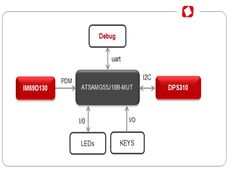
Single-chip 16/32-bit microcontroller; 256\ kB ISP/IAP flash with 10-bit ADC and CAN
 PCB Symbol, Footprint
 Send Inquiry
 Download Datasheet
 SUPPLIERS WHOLESALE PRICE TRENDS
Price comparison from authorized distributors
 LPC2194HBD64 Competitive Prices
EmbedIC has the unique source of supply. We can offer LPC2194HBD64 more competitive price for our customers. You can enjoy our best service by purchasing NXP LPC2194HBD64, Please feel free to contact for the best price of LPC2194HBD64 Controller. Click To Get Quotation
The LPC2194 is based on a 16/32-bit Arm7TDMI-S™ CPU with real-time emulation and embedded trace support, together with 256 kB of embedded high-speed flash memory. A 128-bit wide memory interface and a unique accelerator architecture enable 32-bit code execution at maximum clock rate. For critical code size applications, the alternative 16-bit Thumb mode reduces code by more than 30 % with minimal performance penalty.
With its compact 64-pin package, low power consumption, various 32-bit timers, 4-channel 10-bit ADC, four advanced CAN channels, PWM channels and 46 fast GPIO lines with up to nine external interrupt pins this microcontroller is particularly suitable for automotive applications such as a CAN gateway that connects several CAN busses or a CAN bridge between sub networks at different speeds. Sensors with CAN interface or debugging via CAN are additional applications that need more than two CAN interfaces. It is also an adequate solution for industrial control, medical systems and fault-tolerant maintenance buses. With a wide range of additional serial communications interfaces, it is also suited for communication gateways and protocol converters as well as many other general-purpose applications.
Remark: Throughout the data sheet, the term LPC2194 will apply to devices with and without the /00 or /01 suffixes. The /00 or the /01 suffix will be used to differentiate from other devices only when necessary.
2.2 Key features common for all devices
Mounting Style Surface Mount
Product Lifecycle Status Not Listed by Manufacturer
Lead-Free Status Lead Free
RoHS Compliant
Case/Package LQFP-64_10x10x05P
Manufacturer: Renesas
IC MCU 16BIT 48KB FLASH 44LQFP
Product Categories: 16bit MCU
Lifecycle:
RoHS:
Manufacturer: Cirrus Logic Inc.
IC MPU EP9 200MHZ 208LQFP
Product Categories: MPU
Lifecycle:
RoHS:
Manufacturer: Microchip
IC MCU 32BIT 512KB FLASH 144BGA
Product Categories: 32bit MCU
Lifecycle:
RoHS:
Manufacturer: Microchip
IC MCU 8BIT 8KB FLASH 44TQFP
Product Categories: 8bit MCU
Lifecycle:
RoHS:
Looking forward to your comment
Comment
 Popular Searches
8 Bit MCU, Flash, PIC16 Family PIC16F7XX Series Microcontrollers, 20 MHz, 7 KB, ...
EEPROM 2K 256 X 8 2.5V SERIAL EE IND
System-On-Modules - SOM RCM2200
32-bit Arm Cortex-A53 vision processor with ISP, powerful 3D GPU, dual APEX-2 v...
IC MCU 8BIT 60KB FLASH 44QFP
DSP 20MHZ 44QFP
1
2
3
4
5
6
Product updates, events, and resources in your inbox


Smart System

Traffic Management

Security

Consumer Electronics

Wireless Technology

Robot

Internet of Things

Industrial Control